• The move to the new server is done. There are some software and database maintenance updates in process. This has us passing the hat around to help out. We appreciate any donations. Seriously, even a dollar helps. The payment page may be found here - https://www.audiokarma.org/support.html

Yamaha CR-420 Offset: - 61mV by design!

DC Offset

This idea is not new, but why take an helicopter to go from point A to point B when you can go by foot in less than one minute? If you want to have an adjustable offset, all you need to do is to replace the fixed resistor R407 by a trim pot.

If you use your technique, better to use a larger resistor between the trim pot and the input transistor. A 22k here would reduce the input resistance to ~22k

I plan to measure the AC resistance today. Not looking at the circuit now but thought it was in the feedback loop and would not be 22k. You may be right I will post the measurement results.:scratch2:
 
The problem with this additional circuit is that you can have low offset voltage, by injecting a current in one or the other transistor in the differential pair, but it doesn't change the unbalanced collector currents in the differential stage. This is the unbalanced collector currents which generate distortion in a differential stage.

One of the virtues of measuring the offset voltage in an amplifier like this one is that a low offset voltage is an indication that the collector currents are equal if, and only if, two conditions are met: 1) Both transistors must have the same hFE and 2) the base resistance to ground (or a virtual ground like the output) must be equal (in this circuit for example, R415 must be equal to R401 + R403). The offset add-on circuit is equivalent of changing one of the base resistance, and a low offset voltage with this add-on circuit is a false confidence, offset is low but unbalanced collector currents remains.
 
DC Offset

The problem with this additional circuit is that you can have low offset voltage, by injecting a current in one or the other transistor in the differential pair, but it doesn't change the unbalanced collector currents in the differential stage. This is the unbalanced collector currents which generate distortion in a differential stage.

One of the virtues of measuring the offset voltage in an amplifier like this one is that a low offset voltage is an indication that the collector currents are equal if, and only if, two conditions are met: 1) Both transistors must have the same hFE and 2) the base resistance to ground (or a virtual ground like the output) must be equal (in this circuit for example, R415 must be equal to R401 + R403). The offset add-on circuit is equivalent of changing one of the base resistance, and a low offset voltage with this add-on circuit is a false confidence, offset is low but unbalanced collector currents remains.

So, many of the mid 70s receivers that have this type of circuit, should of done it the way you have listed! What if your circuit feeds both transistors in the first pair through one resistor? I have seen many that do just that. If I send you a circuit, would you look and make suggestions on it to change the DC offset. I'm very interested in your idea's?:scratch2:
 
Last edited:
Excellent bit of sleuthing there, ecluser! I've done this sort of analysis often enough to realize that the wrong value of R407 should stand out like a sore thumb, so I tend to think someone at Yamaha just goofed up one day.

If I was in there playing around, I would add linearizing resistors in series with the input pair emitters, and change the tail resistor to a current regulating diode. These refinements are pretty common in higher-end amps. Hard to say whether you would hear any improvement, though, in a background music application. Cheers!

...and change that input coupling cap to a good plastic film type...
 
Last edited:
So, many of the mid 70s receivers that have this type of circuit, should of done it the way you have listed! What if your circuit feeds both transistors in the first pair through one resistor? I have seen many that do just that. If I send you a circuit, would you look and make suggestions on it to change the DC offset. I'm very interested in your idea's?:scratch2:

I've seen many amplifiers with the offset adjustment on the base of one of the differential transistors. If the objective of the designer was to reduce the offset, it works. But for me it is a lure, it masks another problem.

The option of emitter degeneration with a trim pot is good for adjusting the offset, and increasing the linearity of the differential stage, but you must increase the tail current source if you want to maintain the same transconductance in this stage. This implies that you must also change some components on the collector.

You must understand that if nothing is changed in R405, R407 and TR401 (the Vbe of...), you will always have the same unbalanced collector currents.

There is also the possibility of implementing a current mirror on the collectors of the differential stage.

I changed R407 because I wanted a simple solution and it is something that I do very often in amplifiers.
 
The option of emitter degeneration with a trim pot is good for adjusting the offset, and increasing the linearity of the differential stage, but you must increase the tail current source if you want to maintain the same transconductance in this stage. This implies that you must also change some components on the collector.

Agreed on the transconductance loss, but I've found that simply adding emitter resistors just about equal to internal emitter resistance often improves measured performance despite the gain reduction. Closed-loop gain hardly changes at all, and squarewave edges sometimes look much better.
 
Add DC Offset to Circuit

SORRY I FORGOT TO ATTACH FILE.

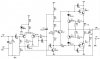
BinaryMike or ecluser, I was wanting to know if you guys would look at the circuit I have attached and see what you would suggest. What is your opinion about the best way to add a DC Offset adjustment to this circuit.

Thanks in advance for your suggestions!:yes:
 

Attachments

  • darl.jpg
    darl.jpg
    84 KB · Views: 58
It has nothing to do with the Yamaha CR-420, but I will nevertheless...

The value of R7 is too large. From the parameters of the components in the circuit, I computed that the ideal value for R7 would be 480 Ohms. You may consider to replace R7 by a 430 Ohms fixed resistor, in series with a 100 Ohms trim pot.

However, this offset will be unstable because it is closely related to the Vbe of T3, which will vary with the temperature of T3.

A better option would be to add some DC degeneration to the emitter of T3, for example add a 100 Ohms resistor in parallel with a 100 uF capacitor. If you do this, the ideal value for R7 would be 1.1 kOhms. Here again, a fixed resistor (1k) in series with a trim pot (200 Ohms) would give you a fine offset adjustment.
 
What is your opinion about the best way to add a DC Offset adjustment to this circuit.

It's probably time to start a new thread on differential input stage optimization, but I would replace the R9-R11-ZD1 network with a PNP current source, and make its reference voltage or emitter resistor variable. But you need to fix up the now infamous Yamaha goof as well. You're apparently shooting for 3.0mA in each side of the input pair, so R7 should be 200R instead of 680R. Not sure why ecluser came up with 480R. Hope it's not my error!

Why did you copy the Yamaha trick of connecting R3 to the C11-R2 node? Do you need to increase input impedance?
 
You're apparently shooting for 3.0mA in each side of the input pair, so R7 should be 200R instead of 680R. Not sure why ecluser came up with 480R. Hope it's not my error!

Yes BinaryMike, you're in error...

Here is how I came up with 480 Ohms for R7:

The zener diode is a 9.1V and the emitter voltage on the differential pair is ~ +0.6V. So, the tail current is 2.6mA

The base voltage on T8 is ~ +1V (when the output voltage is 0V), and the current in R12, R13 is (40V - 1V)/(R12 + R13) = 8.1mA. This is also the collector current of T3. If you consult the datasheet for the BC639, you will find that the Vbe is 0.62V at Ic=8mA

The differential stage will adjust the collector current in T1 in such a way to have 0.62V in R7. More than this critical voltage T3 would be driven too hard and the output voltage would be negative. Less than this critical voltage T3 would be driven insuficiently and the output voltage would be positive.

The objective is to split the tail current in two equal parts, to have the same voltage drop in the base resistors (at this condition the output node becomes a virtual ground, at 0V), AND to meet the 0.62V drop in R7

So R7 must have a value given by:

R7 = 0.62V / (2.6 mA /2) = 480 Ohms

In fact if R7 is different than 480 Ohms the output offset voltage will still be low because the feedback factor is quite large for DC voltage, but the current in each transistor of the differential stage will be different and there will be a small offset voltage.

I think you came up with 200 Ohms for R7 because you forgot the split the tail current in two, and you assumed a Vbe of 0.6V for T3. Am I right?
 
I forgot about that dang zener and just summed the tail resistors. Sorry to put you through all that! I now figure 466R for R7, assuming 0.6V for all Vbe and ignoring T3 base current. Looks like we're essentially in perfect agreement. Feedback at DC is 100%, of course, so any residual output offset will be tiny. I typically see just a few millivolts in breadboard circuits using diff pair transistors chosen randomly from the same shipment, and this is with much higher base resistances.
 
DC Offset

It has nothing to do with the Yamaha CR-420, but I will nevertheless...

The value of R7 is too large. From the parameters of the components in the circuit, I computed that the ideal value for R7 would be 480 Ohms. You may consider to replace R7 by a 430 Ohms fixed resistor, in series with a 100 Ohms trim pot.

However, this offset will be unstable because it is closely related to the Vbe of T3, which will vary with the temperature of T3.

A better option would be to add some DC degeneration to the emitter of T3, for example add a 100 Ohms resistor in parallel with a 100 uF capacitor. If you do this, the ideal value for R7 would be 1.1 kOhms. Here again, a fixed resistor (1k) in series with a trim pot (200 Ohms) would give you a fine offset adjustment.

Could you just replace R7 with 480 fixed and then insert a 100 ohm VR between R9 and the differential pair with the wiper to R9?:scratch2:
 
I think your variable resistor should be larger since R9 is approximately 30 times larger. Your offset adjustment would be very limited with a 100 Ohms trim pot. You must add degeneration on the emitter of T3, or your offset will be unstable.

I don't know if this circuit has been experimented, but I think the bias stage can't provide the necessary voltage to bias the darlingtons. In my opinion R14 should be larger, probably 2.4k or 2.7k. The thermal coupling between T6 and T7 (or T8) must be perfect.
 
DC Offset

I think your variable resistor should be larger since R9 is approximately 30 times larger. Your offset adjustment would be very limited with a 100 Ohms trim pot. You must add degeneration on the emitter of T3, or your offset will be unstable.

I don't know if this circuit has been experimented, but I think the bias stage can't provide the necessary voltage to bias the darlingtons. In my opinion R14 should be larger, probably 2.4k or 2.7k. The thermal coupling between T6 and T7 (or T8) must be perfect.

The circuit is built and has been running for a little over a week. The unit performs great on the test bench and sounds very good. The one thing is that it has about 40mv of offset. The unit has a great square wave at 1k, 10k and 100k. The 100k starts to show ringing on the trailing edge but just a very small amount. T6, T7 and T8 are all mounted on the same heatsink close together. Voltage output into the 8 ohm bench resistor is the same on sinewaves from 10hz - 100khz within .01 VRMS at 23 volt drive. I get my 30ma of bias current at around 65 percent on the pot. Biggest issue is that DC Offset. Before I make any other mods, just replacing R7 with 480 ohms should yield near 0 mv of dc offset? Is this correct? You are also saying to add a 100uf and 100R parallel between the T3 emitter and the -40 power supply, correct? Everything on this board at 1/10 full power runs cool to the touch except for T3, it runs very warm.
 
Last edited:
The 100R trimmer should yield more than sufficient range, with about 64mV across each half when it's centered.

You're right, and I was wrong...

If the actual offset is stable, don't worry about emitter degeneration on T3

Replace R7 and it should lower the offset to a very low value. You may find that you don't need any trim pot on the emitter side of T1/T2

40 mV offset... You meant -40 mV? I computed -25 mV assuming a typical hFE of 100 (these transistors have a rather low hFE) and identical Vbe for T1/T2. How well matched are they in your circuit?

By curiosity, what is the Vbe drop in the TIP142/TIP147 at 30 mA? I figured 1V, apparently it is significantly lower than that.
 
DC Offset Mods

You're right, and I was wrong...

If the actual offset is stable, don't worry about emitter degeneration on T3

Replace R7 and it should lower the offset to a very low value. You may find that you don't need any trim pot on the emitter side of T1/T2

40 mV offset... You meant -40 mV? I computed -25 mV assuming a typical hFE of 100 (these transistors have a rather low hFE) and identical Vbe for T1/T2. How well matched are they in your circuit?

By curiosity, what is the Vbe drop in the TIP142/TIP147 at 30 mA? I figured 1V, apparently it is significantly lower than that.

Thanks again for you guys helping with this! I don't know about the matching of T1 and T2. I guess they are out of different batches. I will test the Vbe drop on the TIP142/TIP147 tomorrow and will let you know. I will also change R7 and let you know the results!
 
DC Offset & Measurements

ecluser:

I built another unit and just finished doing measurements. The T1/T2 has a hfe or 127/139. The vbe of TIP142 & TIP147 is 1.25 Volts at 30ma bias current. The offset is just as you said, it measures -26.6mv! Now I am going to parallel a 1.6k in series with a 220 ohm over R7 to see what happens to the offset. The current R7 measures 667 ohms even though it is marked as a 680 ohms, that will put me at 488 ohms. That is as close as I can get right now. I will post the results!:thmbsp:
 
Back
Top Bottom