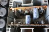
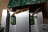
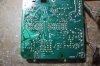
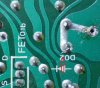
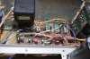
Here is the 'before' picture of the Left Channel driver assembly
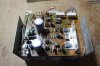
And here is the 'After' picture.

Here is the 'before' picture of the Right Channel driver assembly
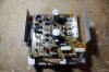
And here is the 'After' picture.
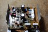
Component changes are as follows
C05, C08 - 4.7µF, 25V electrolytic, replaced with 4.7µF, 63V WIMA Film. (these were a very tight fit).
C09 - 33µF, 25V, replaced with 33µF, 35V Panasonic FC.
C15, C24 - 1µF 50V electrolytic, replaced with 1µF 63V WIMA Film.
C16, C17 - 470µF, 80V, replaced with 680µF 80V Nichicon PM.
VR01 - 100Ω (offset), replaced with 100Ω 25 turn Bourns.
VR02 - 470Ω (bias), replaced with 500Ω 25 turn Bourns.
ZD01 - 27V 1W zener, replaced with 27V 1W zener.
ZD02 - 13V 400mW zener, replaced with 13V 500mW zener.
C03, C10, C13, C18, C21 low value ceramic disk capacitors, replaced with same value Murata C0G/NPO capacitors.
R45, R46, 4.7Ω ½ Watt MOX resistors, replaced with 4.7Ω ½ Watt metal film resistors.
Notes:
All PCB joints 100% inspected with an eyeglass, individual suspect joints were remade. All thermal paste replaced with new. The square brass nuts on the driver transistor mounting screws have had one flat filed clean and were then soldered to the PCB.
Found one bias test point connection (on one driver assembly) was solder bridged to the middle (unconnected) pin, making it easier to short the + & - bias test points - the bridge has been removed. (with sharp eyes you can see this bridge in the picture in post #1)

Found one of the screws that secures the driver & bias transistors to the main heatsink had stripped the thread in the aluminium bracket. Changed this to a machine screw, and added a 'Nyloc nut' to properly secure this thermal path.