• Please note that Audiokarma will be offline briefly for updates early on Monday morning, September 28th.

Blown output on Sony ta-1150d

Command8

New Member
Hi,

I recently recapped a sony ta-1150d. It had mismatched driver transistors and mismatched output transistors and out of tolerance capacitors (replaced mostly with nichicon BP muse, fine gold and wima mks2).

I replaced the output push-pull c1060 and a670 with h1061 and a671. I replaced the noisy driver stage c1124 and a706 with c4793 and a1837. When I turned it on the left side of the output transistors got real hot (i couldn't touch it longer than a second) and blew up, with the ceramic 0.47ohm resistors glowing red hot. I measured again the ceramic 0.47ohm and they now measure 1.1ohm, I'll replace them with 2w metal film resistors.

I'm certain I had the orientation right for the c4793 a1837 replacements, I used my 20$ component tester to make sure I got it right.

What could be the problem?
 
Register to hide this ad
Yeah something is wrong in the Power amp.
index.php

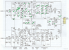
Q409(H1061) and Q410(2SA671) blew up (VT409 & 410 in this schematic from MBuras build thread), those output stage transistors were not complementary as I thought.
2SA671 is a good replacement for the original 2sa670 but h1061 is not a good replacement for 2sc1060.
The amp when testing worked with the DC bias at 10mv. When raising the DC Bias to 25mv (idle current value from the service manual), Q409 blew up, and Q410 smoked.

I'll try replacing all output transistors with D613/B633. It's not an exact replacement however it has better max characteristics than the original transistors and gain bandwidth of 15mhz compared to the original 8mhz.

If those output transistors don't cut it, I'll replace the power amp stage with 2 mono tda7293 amplifier boards I have in my drawer, and install this 12v 2 relay speaker pop circuit.
Max supply voltage on tda7293 amplifier boards is 32V AC. The sony amp has a positive and a negative 35V DC rail.
"Relation Between AC and DC Voltage
AC Volts Χ 1.414 = DC Volts"

35vdc/1.414= 24.75Vac, well within tolerance. I could simply bypass the full-bridge rectifier on these amp modules and supply from the positive and negative rail to the 2200uf filter caps of the tda7293.
 
Last edited:
Finally received all components.
I made a 40watt dim bulb tester from Ikea leftovers.
Spent today measuring D613/B633 hFE values with my mega323 T4 tester to as close as 16 hFE difference between transistors. Carefully matched select D613 that measured 172hFE and all B633 that measured 188hFE.
It really pays to buy 20 transistors to select 8 :rflmao:.
Installed the D613/B633 transistors. Turned the amp on, dim bulb tester dimmed with no issues, so I unplugged the DBT.

I measured the speaker outputs: 35mv on the left channel and 25mv on the right channel.
I'm scared to do the DC bias adjustment. It's how I blew up the output transistors, should I do it with the DBT plugged in?

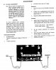
On the Service manual, it shows 2 DMM plugged in tp1 and + speaker terminal respectively for each channel.
I only have 1 DMM, can I do the adjustment with only one?
DC bias adjustmeent ta1150.JPG
 
Last edited:
I did the adjustment, after 20-30 minutes left side started going from 24 to 25 mv to as high up as 2 volts. Basically, on my test speakers, if I press the Speaker button, the left side will THUMP real loud. The right side has also shot up from the mv range to as high as 0.045v. I honestly don't know what could be wrong, I'm still a noob. I'll try spraying the power amp module with cold spray to see if that fixes anything.
 
I do not think those 2SB633/2SD613 transistors will be big enough!
The first clue is on the datasheet: it suggests those transistors are for audio amps with 25W to 35W output, and your amp is 100W!

There is a simple rule of thumb for initial sizing of final transistors for AB output stages.
For the max voltage ratings you want 20% - 30% higher Vce0 than the rail-to-rail voltage in your amp.
The rail-to-rail in your amp is 2X35V, or 70V. So you need a 90V - 100V transistor or so.
For a 8 Ohm speaker the peak current is about 5A. For safety reasons you want a transistor at least with twice that Ic max current rating, as a speaker is a complex load, not strictly ohmic, this causes phase shift, and the actual current will be higher.
So you want to start with 100V 10A transistors. Then you pick your other parameters for the transistors.

Good luck, Peter
 
Thank you, Peter, I was able to find locally TIP31C, TIP 41C, MJE15032/33.
None are rated at 10a but they at least are more than double the original 2sc1060's Ic mac current.

TIP31C and TIP41C has the closest matching hFE (15 - 75) to the original 2sc1060 "A" suffix (35 - 70)
it exceeds original transistor 3A to 6A and is rated for 100v.
MJE15032 according to @dlucy are "excellent replacements with specs far exceeding the 2SC1061".

I'm ordering the tip41c/42c and mje15032c/33c and a set of Boheng 3296 (Chinese bourns clone) 1k trim pots to replace the dc bias pots, as the ageing rubber cement is getting stuck on the tracks.
 
Last edited:
I just discovered another blown transistor, Q552, originally a 2sc945, it was replaced at some point with a c1815gr. I don't have 945 on me but I do have c1815 so I'll replace it.

EDIT: I was wrong, I did have a c945 on me from an old tape preamp project
 
Last edited:
Be careful with saying C945.. 2SC945 is center collector. KSC945 is not center collector unless it has the 'C' suffix.. (KSC945C).
 
Be careful with saying C945.. 2SC945 is center collector. KSC945 is not center collector unless it has the 'C' suffix.. (KSC945C).
Apologies, the replacement is a '2sc945'.
With that transistor in place, the amp now has a visible short courtesy of the DBT. I'm not sure how to progress at this point. The Differential pair on both channels (originally 2sc1632) were already replaced at some point with c1815 (no idea if 2sc or ksc). The only remaining original transistors in this amp are Q304/404(C634A are used as dc bias supply), Q551(2SA678 ripple filter) and Q553 (also part of the ripple filter?). The Q553 was connected from the blown Q552's emitter to its own emitter and base through a 220uf capacitor.

Besides that, I'm unsure as to what to check
 
Last edited:
The final transistors are two pairs in parallel, so the required current rating for a single pair is half that required.
With this in mind, the original transistors are still a bit undersized, no wonder they failed. (This is not the first Sony amp where components were undersized!)
TIP31-32 are OK for drivers, but not adequate for final transistors.
TIP41-42 are OK, but to be really on the safe side triple current rating for the final transistors are preferred.
For this safety reason I would prefer to use the MJE15032-33 transistors as replacements for the finals.

The PA is a feed-back amplifier. If the amplifier fails, manifested by not having close to 0V at the output with no input and/or high current draw, it could come from any stage within the circuit.
When the PA is working fine the output should have no more than 20mV to 40mV DC without audio input.
A way to debug such an amp is to check every and each of the transistors, not just the final and driver transistors, and then the components.
Having a dim bulb tester (limiting the mains input current to the amp) is a prudent way to get to the point where the output DC voltage is close to 0V.
This will protect newly replaced final transistors from blowing up again.
Also, do not forget to set the final idle current when the amp is working.

Regards, Peter
 
Peter, when you mean 0v at the output with no input and/or high current draw. Would this high current draw show itself as the 40w lightbulb in my dim bulb tester not dimming but rather staying on? Or is that just a short in the PA? When the amp is turned on without the PA attached, the light turns on then dimms/fades (It previously did that with the B633/D613). With the B633/D613 it had 35 and 25mv on the outputs yet weirdly enough 8 - 9 mv on the idle current test points.

I'll start measuring all transistors from the differential input until I reach the output stage with my DMM on diode mode :thumbsup:
 
I take you took the above measurements without a speaker.
When checking if the PA is fine without input you do not need a speaker or output load, that would just muddy the results.
35mV and 25mV DC sounds OK on the outputs.
The idle current is a bit low. Still, it suggests that the amp is basically fine, you just need to adjust the idle current.
The service manual for the plain (not D version) mentions 25mV on the idle current test points.
That 25mV is across the 0.47 Ohm emitter resistor(s), that means roughly 50mA idle current in one pair of transistors.
This suggests that you need to adjust the idle current as described in the service manual.

As for the dim bulb test, you have 4 times the 50mA idle current (200mA in total), loading the 70V supply in your amp. That is 14W load. The current (and power) draw of the preamp stages can be neglected compared to this. 14W load in series with a 40W bulb would not give you a fully lighting bulb, it would be dimmed!
A fully illuminated light would indicate a short, most probably in the final transistors.
The idle current test only tests the current in one of the pairs in the final stage. If the final transistors are not mixed, the idle current would be close in the other pair of transistors.

If your DMM does not have hfe (beta) measurement mode also do check for shorts between collector and emitter in the Ohm mode in the transistors, leaving the base open. With a collector-emitter short you still might get OK C-B and E-B diodes.

Regards, Peter
 
I take you took the above measurements without a speaker.
When checking if the PA is fine without input you do not need a speaker or output load, that would just muddy the results.
35mV and 25mV DC sounds OK on the outputs.
The idle current is a bit low. Still, it suggests that the amp is basically fine, you just need to adjust the idle current.
The service manual for the plain (not D version) mentions 25mV on the idle current test points.
That 25mV is across the 0.47 Ohm emitter resistor(s), that means roughly 50mA idle current in one pair of transistors.
This suggests that you need to adjust the idle current as described in the service manual.

As for the dim bulb test, you have 4 times the 50mA idle current (200mA in total), loading the 70V supply in your amp. That is 14W load. The current (and power) draw of the preamp stages can be neglected compared to this. 14W load in series with a 40W bulb would not give you a fully lighting bulb, it would be dimmed!
A fully illuminated light would indicate a short, most probably in the final transistors.
The idle current test only tests the current in one of the pairs in the final stage. If the final transistors are not mixed, the idle current would be close in the other pair of transistors.

If your DMM does not have hfe (beta) measurement mode also do check for shorts between collector and emitter in the Ohm mode in the transistors, leaving the base open. With a collector-emitter short you still might get OK C-B and E-B diodes.

Regards, Peter
Thank you for that insightful comment, Peter. You were correct, the final output transistors were shorted, on the mega 328 transistor tester they mostly show up as diodes so the D613/B633 transistors are coming out. I just received the MJE15032 (all tested 216hFE beta)and 15033 (varies yet mostly 180, 188, 196 hFE beta), I hope this amplifier isn't picky about not very well-matched transistors.

I just remembered the Mega 328 can test transistors and other components in-circuit, I tested most transistors with it:

measured dc bias transistors, they were fine (added fresh transistor compound on their side touching the heatsink where old white crummy compound remained)
ripple filter, q551 and q553 (a678) tested fine
c310 and c410 (10n ceramic capacitors for 35v supply rail to ground) have esr 87 and 122/113uf????
Both 1k bias VR have drifted to 1.3k, replaced both with 1k bourns copy.

differential pair input
hfe 168, 709 mv (q301) hfe 137, 709mv (q401)
hfe 3, 723mv (q302) hfe 3, 724mv (q402)
I will measure q302/q402 out of the circuit, if hfe is still low, will replace all differential pair input.

paraphase amp
Q303 is bad (a1027, originally 2sa735, will measure out of circuit), q403 hfe 82, uf 656mv (a1027)

c304/c404 is bad? (component tester marks it as 732mv diode with 0pf)
r305/r605 (connected to base of q302/q402) is bad, they measure as 47pf in-circuit, will measure out-of-circuit.
q311/q411 are bad (a1027, originally 2sa678), I'm not sure what their purpose is.
 
Last edited:
I tested diff pair input, they are all matched at 211hFE out of circuit, i won't replace them.
Q303 tested fine out of the circuit as well.
Tomorrow I'm receiving another batch of MJE15032/33 from another seller, I'm aiming to match transistors to within 10 - 20 hFE, according to this video(turn on closed captions and you can auto-translate pretty well to your language of choice), as that is how they were originally matched from the factory.

I will measure the rest of below, later today.
c304/c404 is bad? (component tester marks it as 732mv diode with 0pf)
r305/r605 (connected to base of q302/q402) is bad, they measure as 47pf in-circuit, will measure out-of-circuit.
q311/q411 are bad (a1027, originally 2sa678), I'm not sure what their purpose is.
 
If your Mega 328 tester is that Chinese clone transistor and component tester then it can not measure components in circuit!
Take the transistors and other components out of the circuit and measure them that way!
If that is your tester, here is a detailed description of its design and operation, by the original designer:
https://raw.githubusercontent.com/l...-Li-Ion/Doku/trunk/pdftex/english/ttester.pdf

When such amps as yours fail, that is mostly the final transistors and the driver transistors shorting. Chances are you find the problem there.

The role of Q311 looks indeed superfluous. It is an emitter follower, it basically gives low impedance drive to the lower part of the driver-final transistors.
As you mentioned, everyone else in their PA designs manages perfectly well without such a stage.

Here is an excellent treatise about Lin-type power amplifiers (like yours) by Douglas Self:
http://www.douglas-self.com/ampins/dipa/dipa.htm

Regards, Peter
 
Last edited:
Thank you kindly for the site, Peter. I have read Douglas Self's 'Small Signal Audio Design (2020)' I very much liked his addition of tape machines, it was a very intriguing read regardless of my lack of understanding of most of the content.

Replacing the output transistors with MJE I had on hand fixed the shorting issue you noted.
I took and measured all the D613/B633 transistors, nothing shorted on the right channel, on the left channel 3 out of the 4 transistors shorted (being only identified on my Chinese lcr-t4 as diodes).
This is becoming a recurring pattern, the left channel has repeatedly blown out the output transistors.
After turning the amp on after 20 seconds I measured the dc output: -0.08VDC on the left channel, -0.005VDC on the right channel.
Idle current after 2 minutes turned on is -45mv on the left channel and 15mv on the right channel.
From what I can observe in 10 seconds the right channel is able to lower its voltage to what is expected whereas the left channel starts up slow and takes a while longer to lower its voltage, given that, any ideas as to what component might be defective?
I've tested just about all the transistors out of the circuit and they all tested fine or at least not broken. To find this gremlin, I think I will need to measure voltages at the indicated points on the PA diagram in post 3.

checked components 1150.png
I've crossed out all the components I've currently checked, measured out of the circuit and/or replaced in the attached image. C303 is 3pf green mylar or ceramic capacitor and I can't measure it, either with my Aneng DMM or my LCD T4 which should have enough resolution for it, I tried measuring another 3pf ceramic capacitor with no success.
 
The thermal behaviour of the final transistors are "governed" by the Vbe multiplier, by VT304. Those transistors are usually mounted on the heatsink.
Are those transistors the same type for both channels? Are their mountings from thermal point of view similar?
A critical component in the bias current setting are the VR301 pots. If those pots fail that could have catastrophic consequence for the final transistors.
The design of that pot in the Vbe multiplier circuit is not "fail safe", for a fail safe design the pot should be between the base and emitter, if a pot fails in that position the Vbe transistor gets fully open, reducing the bias current to zero. You can read up on this and you also might want to modify the circuit accordingly.
I looked at the other thread about the "building" of that amp. Do I see it correctly from the pictures that the final transistors are in sockets and not soldered?
A socketed power transistor is not as reliable as a soldered in one!
I would check out these components.

The 3pF cap is most probably ceramic and is not that critical, if it is not shorted I would take it as good.

Regards, Peter
 
Are those transistors the same type for both channels? Are their mountings from thermal point of view similar?
I looked at the other thread about the "building" of that amp. Do I see it correctly from the pictures that the final transistors are in sockets and not soldered?

Both VT304 are the same (2sa633) mounted on the heatsink edge, I added a bit of fresh transistor compound on both transistors. facing the heatsink.
The VR301 pots have been replaced with modern 10 turn 1k pots. I will look into repositioning the pot and modifying the circuit as soon as the circuit is fixed :thumbsup:.

I looked at the other thread about the "building" of that amp. Do I see it correctly from the pictures that the final transistors are in sockets and not soldered?

Correct, they are in fact socketed, when I take the output transistors out, I will bend the edges that make contact with the transistors to give the connection more rigidity.

I have measured out-of-circuit this time a lot of resistors and transistors (and luckily, the driver stage transistors weren't shorted).
checked components 1150.png

I forgot to add a picture of the power amp, it certainly looks more colourful than before. I've been keeping track of which components I've checked already with a golden marker. Of note, VT303 (Pre-driver originally 2sa678, on this amp came as A1027) on the left channel, the collector is supposed to give out 1.25v, I have measured 1.6v. should I consider replacing them? I'm not sure what else could cause the -0.08v that plages the speaker output.
Power amplifier recapped and components checked with gold sharpie.jpg
 
VT303 is the VAS (voltage amplifier stage) transistor. The voltage on its collector is derived from the output DC voltage, which is supposed to be 0V, and the sum of the two Vbe voltages of VT309, VT307, and VT305. Those Vbe voltages are about 0.6V.
There is also the voltage across R313, which should not be much.
The 0V at the output is maintained by the DC feedback from the output to the input differential amp (VT302) and by the fact that the base of VT301 is held at ground level by R302.
Do measure if the base of VT301 is indeed at 0.015V according the schematics.
Do measure the voltage at the base of VT302, it should be pretty close to the voltage at the base of VT301.
Do measure the Vbe voltages of the final and driver transistors.
This will give you an answer where the excessive voltage at the collector of VT303 comes from.
If you think about it, this is just like how an op-amp is biased, a Lin-type audio amp is basically a power op-amp.

There is also some protection circuit implemented by VT553 and VT552. Those transistors could interfere with the DC output voltage of the amps.
Those transistors open if their base is 0.6V beyond ground, and that point is given by two resistors from the outputs of the two channels, R555, R556.
Do measure the voltage at the base of those two transistors, it should be about 0V.
If push comes to shove, disconnect that protection circuit from the rest of the amps, from the base of the driver transistors, by removing diodes VD559, VD560, VD55, VD557, VD558, VD556 temporarily.
The original, non D-version of the amp did not have that protection circuit.

Regards, Peter
 
Last edited:
Back
Top Bottom