• The move to the new server is done. There are some software and database maintenance updates in process. This has us passing the hat around to help out. We appreciate any donations. Seriously, even a dollar helps. The payment page may be found here - https://www.audiokarma.org/support.html

Denon PMA-900V Troubleshooting

Easy enough, thank you. However, few questions:

Where do you know to pull the voltage (2V above) off of the schematic? (I'd like to learn stuff like this so as not to ask the same type of question again)

I must have had the PDF cutting off part of the part description on these when I looked earlier. The BOM lists R551,553 as: 100 ohm, +/-5%, 1/4W, Carbon (NBS). R559 is the same specs but (NBF).
- Any idea what NBF vs NBS is? Physically they look the same except the R551 and R553 are oriented vertical off the board and R559 is horizontal.
- All are axial resistors. Can I just order axial across the board and bend the leads to orient vertically on R551 and R553?

Finally, the schematic BOM lists Carbon for these, whereas other resistors list as Metal Oxide Film. Still good with ordering Metal Film mentioned above?
 
Carbon film is cheaper than metal film but the latter handles overload much better and is more stable. The 2 V is not listed on the schematic but it is the combined diode drop of the power transistors. Actually, this voltage is nearer 1 V. Thought it was before the driver transistors. Hasty, hasty... But it was just to illustrate it doesn't have to work very hard. When idle in any case. Its main task is to remove base charge from the power transistors in order to switch them off faster during heavy load. Hence the 0.5 W rating. If the manual sez 1/4 W that will be fine. I try to err on the safe side but rarely look in parts lists. Which should not be taken as gospel in any case.
 
Alright, good to know, thanks for the explanation. For as cheap as the resistors were in comparison to the minimum shipping charge, I bought both carbon film and metal film on the 100 ohm resistors. Also stocked up on a handful of others that I may never use but it was cheaper than the shipping charge.

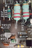
No harm installing these in the vertical for R551 and R553 right? Just bend the lead to fit and not short to anything else? Here's a pic of the R559 horizontal vs the R553 in the vertical (burnt casing example on R559 that I did not see when initially scanning the board at the start of this).
upload_2021-1-22_16-37-59.png
 
No idea what happened at your end. Maybe a piece of wire got stuck somewhere and came dislodged after pulling the fuses. You may want to check for something like that first. I never like incidents like that. Makes me very nervous.

Now you've got relay click test whether voltage across R559 is sane and adjustable with VR5. Should be around 1.0 V. Then turn it to its lowest and power off. Wait for the capacitors to discharge (experience!) or help them with a low value power resisor (100R/5 W is perfect). Install the power transistors. Double check your work, test for shorts, check the correct transistors in their respective places, stuff like that. Do one channel first, disable the other (pull its fuses).

Alright, parts arrived today. Going to be replacing R551/553/559 then check voltage across VR5 as stated in quote above. If within reason, I'll continue down the remaining direction above:
- VR5 adjust to lowest, power off
- capacitor discharge
- power transistors install

Advise if thoughts on that have changed.

If all is checking out after power transistors install, then test bias and DC offset (I assume bias will need adjustment and will follow the idling current adjustment from the service manual, pretty straightforward). If DC offset is out of whack, will need some advice there.

If bias and DC within reason, then sound check. Sound right?
 
Okay, R551/553/559 back in. Voltage across R559 was 0.380 V with VR5 turned all the way down, and 1.370 V with VR5 turned all the way up. Power transistors back in, all measured within reason when checking parts I had touched.

For testing and adjusting bias, measurements and adjustments made at 10 second, 5 minute and 15 minute marks per the service manual. Results of both left and right channels were same:
- Nailing the 10 second at 0.4 mV was touchy but got close enough to the 0.4 mV
- 5 minute reading came in about 3.9 mV on both channels, adjusted to 5.0 mV on both
- 15 minute reading came in at 5.6 mV on both channels, adjusted to 8.0 mV on both

Now, DC offset measurements:
- Right Channel (untouched channel) measurement floats between 5.6 mV to 6.6 mV (could be relatively cheap DMM I have or just normal for some float)
- Left Channel measurement floats between 65.0 mV and 66.5 mV

So, now to reconcile the DC offset on the Left channel, or other "to-do" items unrelated to DC offset. I don't see adjustment pots/variable resistors for adjusting DC offset like the service manual has for the idling current/bias using VR5 and VR6.

Please advise on where to go from here, thanks again to all for the help in working through this!
 
65 mV is a bit high-ish. Check the output of the voltage amp (junction of R435/7) and compare with R_Ch. Otherwise don't bother. You cannot adjust DC offset in this amp. Either the JFETs at the input, IC5 or the associated electrolytics could cause this.
 
Alright, I kind of had to take a stab at what the testing intent was, but think results of voltage across R435 and R437 will probably give you the info you need to give me further direction on next steps:

Tested voltage across following resistors to compare L and R channels:
LEFT:
R435 / 0 mV
R437 / 0 mV
RIGHT:
R436 / 45.5 mV
R438 / 47.9 mV

Prior to voltage test above, tested resistance on the same below:
LEFT:
R435 / 23.1 ohm
R437 / 22.7 ohm
RIGHT:
R436 / 22.8 ohm
R438 / 22.9 ohm

Also took a stab at what I believe would be the JFETs you mentioned but probably need some direction on correct way for testing each of the transistor types listed below:
Diode test for all results below:

RED to GATE, BLACK to DRAIN
LEFT
TR401 / 0.655 V
TR403 / 0.654 V
TR211 / 0.143 V
RIGHT
TR402 / 0.653 V
TR404 / 0.653 V
TR212 / 0.158 V

RED to DRAIN, BLACK to GATE
LEFT
TR401 / 0.863 V
TR403 / OL
TR211 / 0.158 V
RIGHT
TR402 / 0.853 V
TR404 / OL
TR212 / 0.182 V
 
Last edited:
Alright, I kind of had to take a stab at what the testing intent was, but think results of voltage across R435 and R437 will probably give you the info you need to give me further direction on next steps:

Tested voltage across following resistors to compare L and R channels:
LEFT:
R435 / 0 mV
R437 / 0 mV
RIGHT:
R436 / 45.5 mV
R438 / 47.9 mV
Oh, did not see that one coming... R435/7 carry no current. No wonder you get offset. Amazing you get anything at all. This changes everything. Test voltages around Tr411 and 415 as per manual below. One of these could have gone phut. Output transistors Tr417/9 are also suspect. Even more so because you do get amplification even with offset. Whatever causes this should be apparent with the eight voltage readings you are going to produce.

All your other measurements are OK.

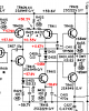
denon_pma-900v_sch_crop.png
 
Test voltages around Tr411 and 415 as per manual below.

View attachment 2112396

Thank you for the manual/screenshot, definitely helped to clarify!

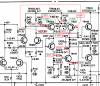
Leader arrow of each measurement strikes through the red highlighted voltage values you had posted in the manual (except Base leg measurement of TR411, that one is boxed, I think I got that right??). Generally all measurements were taken from chassis ground to identified BCE leg of the associated transistor except for the voltage between R425 and R427. I tested across R425, R427, and R423 (listed below) and also tested the Emitter legs of TR409 and TR411 (green on attachment below) which is likely redundant.

R425 / 0V
R427 / 0V
R423 / 43.7V

So, R425 and R427 are shot. I would guess based on no voltage drop/gain that TR411 and TR413 are shot? I may be WAY off on that, just trying to learn and see if my assessment is anywhere close to accurate. TR411 very suspect, TR409 less suspect....all I'd be confident in is R425 and R427 being shot though.
upload_2021-1-28_11-42-12.png
 

Attachments

Wa-wa-wa-waaaaat?!?!? These values do not make any sense whatsoever! Are the supply rails OK at +/-60 V?
 
Wa-wa-wa-waaaaat?!?!? These values do not make any sense whatsoever! Are the supply rails OK at +/-60 V?

Hold up, I was so far off on my hope at an assessment....started testing resistance values and R425 and R427 are likely fine. R423, R429, R431, R415, R413 are visually fried/discolored...see pic, mirror of LEFT channel to the top, RIGHT channel to the bottom. Compare color of resistors between fried LEFT (brown) and good RIGHT (green). Measured the full LEFT channel resistors of this area of the circuit. Will post measurements in a minute.
 
The schematic (and also the 700V) is missing the connections to the supply rails from the PSU to the voltage amp stages (the one with the 4xx numbers). The 500 is OK. The layout is useless...
 
Not in any particular order, resistors in this part of the board measured out as follows:

R425 / 4.7 ohm
R427 / 4.7 ohm
R423 / 35 Mohm
R429 / 22 Mohm
R431 / 10.8 Mohm
R415 / 35 Mohm
R413 / OL
R419 / 10 ohm
R417 / 10 ohm
R421 / 0.992 Kohm
R437 / 23 ohm
R435 / 22.2 ohm
R439 / Measured all over 35M down to about 63K, nothing steady always climbing/falling
R449 / 560 ohm
R409 / 331 ohm
R407 / 1.933 Kohm
R405 / 1.933 Kohm
R403 / 100 ohm
R411 / 2.831 Kohm
R491 / 227 ohm
R445 / 116 Kohm and climbing slow
R423 / 16 Kohm
R441 / 90.2 Kohm and climbing slow
R401 / 220 ohm
 
Looks like you're facing blanket replacement of about 10-15 components. Anything semiconductive even close to a fried resistor is suspect. Don't even bother testing them after removing them.
 
Wow, what a carnage...

Ha!...it was so unsuspecting as they kind of blended with the factory tan colored resistors, just a little charred. Pulling and testing the following ones that are visibly fried. If any of the other in circuit resistance measurements seem suspect and should be added to this PULL list, let me know.

PULLING:
R423 / 35 Mohm
R429 / 22 Mohm
R431 / 10.8 Mohm
R415 / 35 Mohm
R413 / OL
 
Looks like you're facing blanket replacement of about 10-15 components. Anything semiconductive even close to a fried resistor is suspect. Don't even bother testing them after removing them.

Fair enough, more components help me feel better about the $11 shipping cost...kidding but not kidding. I'm committed to this as it's basically like buying a text book for me, learning a lot along the way.

So, any resistor not close to the resistance value in the service manual is coming out. Some of the high value resistors that had slow climbs to them seemed to test similar as the RIGHT channel ones...should RIGHT channel be used as a benchmark comparison before pulling?

R425 and R427 are not in the parts list that I can find by the way, listed as 4.7ohm on the schematic, not sure of wattage though. You had explained the calculation previously but I still don't understand how to determine the V value from the schematic. I would guess at 1/4W similar to R423 but that's just a guess.

What about determination of transistors, capacitors, diodes or other for replacement? I'm in it for the long haul, thanks for your help and I hope you stay along for the ride.
 
Back
Top Bottom