• The move to the new server is done. There are some software and database maintenance updates in process. This has us passing the hat around to help out. We appreciate any donations. Seriously, even a dollar helps. The payment page may be found here - https://www.audiokarma.org/support.html

Kyocera A-910 Restoration & Information Thread

Connor G

Ear conditioned
Subscriber
Hey fellow AKers,

It’s been a while since I posted a new thread about a piece of gear, so I find it fitting to do just that now that I have recently acquired a beautiful Kyocera A-910.

Kyocera has been on my radar for a few years now, especially gear from the 910 series. I’ve wanted an A-910 for a few years, but they are so rare that the thought of ever owning one had quickly diminished. Fast forward to a few months ago, my friend @Will_Emanuel picked up an A-910 local to him very cheaply. Seeing how well built the 910 was through his photos, my desire for an A-910 was reignited and it quickly moved up on my list. Well, after a couple of weeks, an A-910 was listed about 20 minutes from me for a price I couldn’t refuse! It’s crazy, as Kyocera’s 910 series is extremely rare in the US.

The 910 is of the best constructed amplifiers I’ve personally had through my hands, and that’s not a small feat.
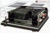
The entire bottom portion of the chassis is made of a special ceramic composite material which was said to reduce resonance and vibration from transferring into the 910. It adds a ton of weight and makes the 910 a very heavy integrated amplifier.

BCA110FC-5DAA-4F20-8A5A-18B8CADBC78A.jpeg
9CBDFB33-CC9A-4064-93E7-74F6CD5A56AB.jpeg
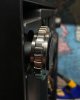
Externally, every piece of the 910 is made of metal. Everything from the knobs to the accents. It’s astonishing. Even the front feet are made from solid aluminum, and are adjustable.
5C2159B7-F1E8-4610-81A9-D3FB80CB4F5D.jpeg

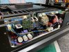
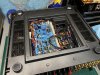
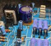
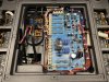
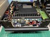
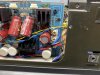
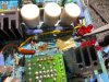
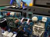
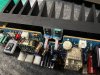
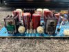
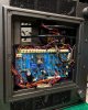
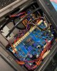
I removed the bottom panel and snapped some photos of the power supply and Sanken outputs. I’ve yet to see photos of the power supply section of the 910 on the internet, so these may be a first. Overall, it is cleanly laid out and the wiring is neat. The boards in the 910 are covered with the typical 70’s/80’s corrosive glue, so that will have to be dealt with.
4D4814C6-681E-4333-8EF3-0C5EEB200BE3.jpeg B89F4696-236D-479C-AC3E-8EEC5F9E12E6.jpeg 553C6FDE-5EA7-4BA3-9794-BB14F98C3CDA.jpeg

The main point of this thread is to have an archive of information available for people who are interested in the A-910. There is very little information available online, aside from a page from TVK, and a few other dead threads here on AK.

I plan on restoring my 910 from top to bottom in the coming months. It’s going to be quite an undertaking but I know that I am more than capable of taking it on. I will be sure to document the process here in this thread.

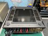
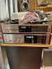
Here are a couple pictures of my A-910
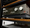
7E601344-1046-433C-B894-949BE8548E73.jpeg 9280F432-F66F-4212-B472-2AA9A20B5B2F.jpeg

Anyone here have any of the Kyocera 910 series? I’m keen on seeing how many people are aware of them.
 
Last edited:
Register to hide this ad
That's a clean looking unit. Had no idea they made these. What year(s) were these available?

Interested to see how you like it.:lurk:
 
They are beautiful integrated amps. I’ve never seen one come up for sale locally but they are definitely on my very short list of “must buy” gear.
 
I’ve never seen one come up for sale locally but they are definitely on my very short list of “must buy” gear.

I just finished a A-710. I looks very similar to the 910. The 710 is very nice and easy to work on. If you can't find a 910, the little 100 w/c 710 might fit your need too.
 
I just finished a A-710. I looks very similar to the 910. The 710 is very nice and easy to work on. If you can't find a 910, the little 100 w/c 710 might fit your need too.

I’m sure it would. I have seen zero Kyocera stuff for sale and I’ve had searches up since seeing one of these threads years ago.
I’m an integrated guy and love my Japanese market Yamaha A-950 but have been intrigued by these for a while.
 
I really like the layout. Some thought was put into ease of repair also. I've built a couple Tube amps with screw terminals and spade connectors added to the circuit boards. It makes it much easier to remove and repair anything on the boards if needed.
 
Work on the A-910 has begun...

Preface:

I've had some spare time this past week, so I decided to start working on the A-910. This is going to be a thorough restoration where no stone will go unturned.
There are no other posts online about the A-910 in terms of servicing, so I plan on posting the restoration process in detail. Please bare with me as I am a full time student, and also working to make ends meet. This will likely be a very slow process, as I will be working on this unit in my free time; usually during the weekends. I am also a very meticulous worker, so I will be spending a lot of time doing some things that other people may overlook. I am doing this as a labor of love, as this is my personal unit. I haven't entirely decided whether or not I will be keeping the A-910 though. I have wanted one for my collection for the past couple of years, but being in the situation I am in now, I am not sure if I can justify yet another amplifier in the collection. I may have to thin the herd in other areas though, as I really like this amplifier.

Overview of work to be done:

The Kyocera A-910 will require a fairly straightforward, yet comprehensive restoration. It suffers from many of the same issues that similar amplifiers of this era do. Issues like bad soldering and corrosive glue are here in spades. Old capacitors, dirty switches and potentiometers, carbonized relay contacts, crusty adjustment trimmers, messy wave soldering flux residue... You get the idea. All of these issues need to be addressed to assure the stable working condition of this amplifier for the next few decades. Like I said before... comprehensive.

A small rant about the misnomer of a "restoration":

One of my biggest pet peeves in the audio world is the common practice of dramatizing work done to audio gear. This is usually done to artificially and disingenuously drive the price of gear on the second hand market up. Many people believe that a "restoration" only includes spraying deoxit into the UI potentiometers, cleaning the faceplate, blowing dust bunnies out of said piece of equipment, and less frequently, a basic recap. This is very far from the truth, and usually puts honest technicians like myself in a bad spot when confronted about why it takes as long as it does for a thorough restoration. Audio gear of this age suffers from much more than the typical bad capacitors, and usually requires specialized service to guarantee the stability of the unit overtime. Again, the term comprehensive servicing comes into play again. Remember this.

What I believe a "restoration" is:

In my eyes, a restoration is where a piece of equipment is brought back to factory specifications and working condition both inside and out. This is accomplished by addressing every issue both known and observed. Things such as removing corrosive glue, reflowing and defluxing circuit boards, replacing capacitors and known problematic signal transistors and regulators, addressing heat related issues such as PCB and trace damage, remounting outputs and drivers on new thermal interfaces, and even a thorough cleaning. There are more steps to take than this, especially depending on what it is to be worked on, but you get the idea. There is much more to a "restoration" than what most eBay sellers would lead you to believe.

Back to the topic at hand... The A-910.

This past weekend I started work on the 910. I decided to attack one part of the amplifier at a time. I do this to make it easier to isolate possible issues that could be created by working on the amplifier. The saying "Show me where you were and I'll show you where the issue is" is very true. It's always best to work in small steps and avoid working on everything at once.

The A-910 takes up about as much bench real estate as I can offer. It is 17"x6"x17" and weighs an impressive 50 pounds. Much of the 910's weight comes from the massive transformer, and the ceramic composite base. To ease in moving large equipment around on my bench, I use a small platform with caster wheels mounted to it. It makes it much easier to rotate equipment without having to strain and risk damage.

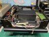
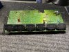
As you can see in the following photos, the A-910 seems to be a relatively straightforward design. Power supply smack in the center, main amplifiers on either side, preamp section toward the back, and interface circuitry to the front. The amplifier cards are mounted directly to the heatsinks, which are then mounted to the CCR base with four screws. All of the wiring is attached to the corresponding PCBs with screw terminals and header plugs. No annoying wire wraps anywhere to be seen. This makes disassembly and reassembly relatively easy. I take photos of the wiring before removal so I have a reference as to how to reattach them when the time comes.

IMG_8583.JPG IMG_8584.JPG IMG_8586.JPG IMG_8593.JPG IMG_8588.JPG IMG_8594.JPG IMG_8595.JPG

The next post will be of the power supply rework. Stay tuned.
 
Last edited:
Power supply section:

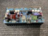
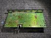
Getting to work on the A-910, I decided to start with the bottom power supply board. This board is mounted to the bottom side of the CCR chassis, and supplies power to various parts of the amplifier. There are many wires leading to and from this board, so noting where each wire goes upon removal of the board is of utmost importance. All of the wires are attached either by header plug, or by screw terminal. Kyocera added a nice touch by soldering the very tip of each wire leading to the screw terminals, mitigating the risk of having wires fray and short on one another.

IMG_8595.JPG

IMG_8616.JPG

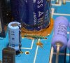
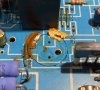
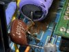
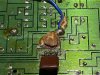
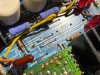
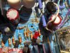
Upon removal of the power supply board, I spotted a few issues right off the bat. One of the issues immediately apparent was the use of corrosive glue which was used to hold down a large capacitor on the board. The glue had creeped to a nearby jumper and had started corroding it. I removed the capacitor, cleaned the glue residue, and replaced the jumper with a new one. Luckily, this was the only area on the power supply board which had corrosive glue used on it. Unfortunately for many other areas in the amplifier, this is common. Removing corrosive glue and repairing damage it causes is easily one of the most time consuming processes there is to do when servicing equipment like this. Many times the glue will cause irreversible damage to components like semiconductors. This leads to the mandatory removal and replacement of said components to avoid issues down the line.

Mike over at Liquid Audio has an article about corrosive glue which is helpful for people who haven't heard of it before.

IMG_8676.JPG IMG_8677.JPG IMG_8678.JPG IMG_8679.JPG IMG_8680.JPG IMG_8681.JPG

Overall, the PCB was in good shape, but needed attention. There were a few capacitors to replace, as well as many solder joints that needed to be touched up. The main power relay was also carbon fouled due to high current arcing. Addressing these issues now is a good thing to do even though the power supply was working correctly.

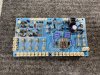
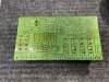
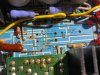
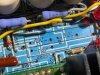
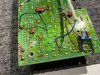
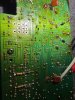
Here are a couple of photos of the board, before reworking. Note the mass amount of flux present on the circuit board, as well as all of the cold solder joints.

IMG_8614.JPG IMG_8615.JPG
 
Power supply section cont'd:

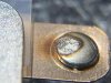
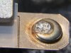
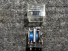
Generally, I am not a fan of sanding or polishing relay contacts, as doing so will remove the protective coating on the points. In some instances though, doing it is necessary.
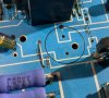
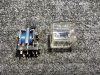
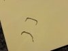
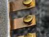
The main power relay on the PSU board had large amounts of carbon fouling, as well as damage to the points from high current acing. Disassembling the relay to clean the points needed to be done in order to ensure a low resistance connection. As you can see, the damage was pretty significant.

IMG_8682.JPG IMG_8683.JPG IMG_8684.JPG IMG_8685.JPG

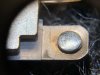
After opening the relay and cleaning the contacts, I decided to adjust the angle of the arms in order to allow the points to sit flatter on top of one another. From the factory, the points sat on top of each other at a relatively bad angle, making it so the area in which the points actually made contact with each other was very small. Adjusting the arms should increase contact area and theoretically reduce resistance.

IMG_8686.JPG IMG_8687.JPG IMG_8688.JPG IMG_8689.JPG

I am actually surprised that a relay which utilizes bifurcated contacts wasn't implemented into this circuit, especially considering this relay seems to be switching high voltage / current. Bifurcated contacts increase reliability, which is important for a relay in this position.
 
Power supply section cont'd:

After recapping the power supply board, removing the corrosive glue, and repairing the relay, I decided to reflow and deflux the entire board.
Reflowing and defluxing PCBs is also another very time consuming process, especially when done right. Many people often times overlook many questionable solder joints, and not to mention, fail to deflux the board after working on it. I like to deflux circuit boards for a few reasons.

1: Defluxing makes it very easy to inspect your work and make sure there aren't any solder bridges or broken traces. With a thick coating of flux on a circuit board, it makes it almost impossible to be able to get a good look at all of the joints and connections. Once it's defluxed, you are able to see every detail.

2: If your flux is acidic, it's best to remove it from the PCB entirely. Most flux used today is non-acidic, so it won't attack or corrode traces. But I have seen my fair share of damage caused by acidic flux left on circuit boards, so I make it a habit to remove it all. It doesn't hurt.

3. It makes your work look much better. When I open an amplifier that's previously been worked on, I usually see gobs of flux coating the circuit boards. This tells me the previous person to work on the piece of equipment didn't really care about the final product, or was rushing to get the job done. When I finish soldering, I always like to deflux, even if it adds extra time to the job.

I use an acid brush to apply flux to boards I am reflowing. I also add solder to any joint that needs it. Adding flux to every joint makes the process go much faster vs relying on the flux in the solder you are applying. I get shiny joints that look great every time this way.

IMG_8690.JPG IMG_8692.JPG IMG_8693.JPG

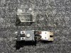
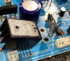
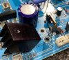
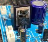
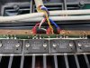
The last thing to do was to remount the TO-220 transistor on a new silicone thermal interface. I noticed that all of the thermal compound in this A-910 was dry as a bone, so replacing the mica and grease with silicone pads is what I will be doing with every transistor. There is a never ending debate about whether or not silicone pads are as good as the standard mica and grease. My view is that if you use high quality thin silicone insulators, they will be very close in terms of thermal transfer when compared to mica and grease. The efficiency of mica and grease also depends heavily on how much compound you use, and how thick your mica insulator is. I use silicone in almost all of my restorations and projects, and have never had a single issue. Even when used in class A driver and output sections that get very hot. Silicone pads are also much easier to install, and in turn result in a much cleaner end result.

IMG_8695.JPG IMG_8696.JPG IMG_8697.JPG

The final result is great. After reworking the PCB and installing it back into the chassis, I redid the wiring and made it look much cleaner than stock. This will make it much easier to remove the board in the future if need be. I'm really happy with how it came out, but this is only one small piece in the puzzle that is the A-910. I have since started working on the amplifier sections, and they are proving to be much trickier to work on as they are filled with corrosive glue. I will update this tread as I get closer to finishing them and I will be sure to take many detailed photos for all of you who are interested. Stay tuned!

IMG_8694.JPG IMG_8707.JPG
 
Left amplifier section:

I pulled the left hand amplifier module from the 910 the other night and did some preliminary inspection. The amplifier PCB is mounted to the heat sink with 4 screws, and the heat sink assembly is held to the CCR chassis with another 4 screws. There are a few wires attached to the PCB with screw terminals, and a few other with the header plugs. 4 more wires are located toward the bottom of the PCB that are attached to the bus bars with ring terminals. After removing the wires and the 4 screws that hold the heat sink to the chassis, the module pulls straight up and out.

67D5149F-DEFB-45D8-8D6E-B5F9CFE47FF3.jpeg AA421965-54A6-4CE7-9B5E-4B3BA04A6C85.jpeg B170798D-FE5C-4A3C-B89B-C1BD7D9F0DAA.jpeg 4DA8EC52-4EEC-46B2-A368-6276EC0A53B3.jpeg EB71DC60-360D-479D-81BC-EC45542275F0.jpeg EFDF3BE2-4F73-495C-B353-B573B85E4FA4.jpeg

Overall it has been very easy to access and work on the boards in the 910, mainly because there are no wire wraps or soldered wires. Everything is easily accessible and removable which is a huge relief.

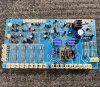
Here is one of the amplifier modules. It’s mounted directly to the heat sink, and the transistors are then soldered to the board and screwed to the heatsink.

25F5DEF4-50D5-4F96-9439-5B1D1ED64C25.jpeg 0B7857AF-68D7-4CE5-9BC5-6C4B3B47446F.jpeg
 
Last edited:
Left amplifier section cont’d:

After careful inspection, I found multiple issues with the amplifier section that will need immediate attention. Tons of corrosive glue, lots of bad soldering, and leaky capacitors.

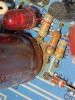
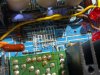
There is a ton of corrosive glue that was used on the amplifier cards, mainly used to hold down the large Elna capacitors. Other areas where it was used was on the bottom of the PCB to hold components like Diodes and capacitors down. This glue has migrated to nearby components and has caused a lot of corrosion. It’s even caused quite a bit of corrosion on the PCB traces.

57927DBB-4461-4462-A99C-40787CA328BC.jpeg 60B5D648-B6B9-4C2A-977D-F528D34239F8.jpeg BF47835C-DEDB-4B7D-B293-457794446D5F.jpeg 437BB1CC-F81F-4EBF-8BD5-8CB65E801B9A.jpeg 0E0ED5AE-AF82-4119-9557-8DAF8B1CAA87.jpeg 00C9D9C6-6A67-4CF9-84AA-5EFF3B05927E.jpeg 74606BDA-D25E-4FCD-A583-4C3C36FA6E85.jpeg 7C442806-87F3-4AC4-8552-230EB47564EB.jpeg 7FCC255C-A277-437F-8882-C6916D605C2B.jpeg A564EE03-724E-4E43-A6FC-AC88BE1336C4.jpeg

I’ve since started removing this glue and cleaning much of the corrosion up. It’s easily one of the most time consuming jobs to do which slows the process down significantly.
 
Last edited:
Iirc these amps have a mosfet driver stage with the big SanKen outputs… would like to get one if i could ever find one in 240V - these are rocking horse poo
 
Left amplifier section cont’d:

I've been working on the left hand amplifier section on and off for the last couple of weeks and managed to finish it yesterday. Being in Massachusetts, we are currently being hammered by a large snow storm. I am snowed in right now, so what better time to add an update to this thread about my progress on the 910 thus far...

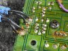
Starting work on the left hand channel involved cleaning all of the glue and corrosion on the PCB. This was a very time consuming process that took the better part of 3 hours. Many large capacitors on the board were held down with copious amounts of the nasty glue, which had migrated to other components. Luckily, the corrosion damage was minimal, but was still a hassle to deal with.

photo_2022-01-29_15-43-14.jpg photo_2022-01-29_15-43-18.jpg photo_2022-01-29_15-43-20.jpg photo_2022-01-29_15-43-25.jpg photo_2022-01-29_15-43-28.jpg photo_2022-01-29_15-43-30.jpg photo_2022-01-29_15-43-33.jpg photo_2022-01-29_15-43-35.jpg

This was one area out of many on the left hand amplifier module. After removing the glue, cleaning the board with isopropyl alcohol, and installing new jumpers, it looks as good as new.

The output relay was surprisingly clean and had no corrosion or pitting on the contact points. No servicing was needed!

photo_2022-01-29_16-03-45.jpg photo_2022-01-29_16-03-54.jpg
 
Last edited:
Left amplifier section cont’d:

Some more pictures I took while removing glue, reflowing, replacing capacitors, and redoing the wiring on the board. Kyocera used a lot of very long wiring on the PCB which could act like an antenna and cause oscillation - especially in a high bandwidth amplifier like this. I shortened the wiring to mitigate this issue from happening. It also looks better this way :)

photo_2022-01-29_16-05-02.jpg photo_2022-01-29_16-05-12.jpg photo_2022-01-29_16-05-18.jpg photo_2022-01-29_16-05-21.jpg photo_2022-01-29_17-07-38.jpg

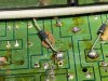
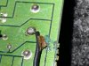
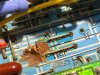
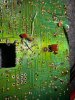
Here is one area of the PCB that was eaten away by the corrosive glue. I attacked the corrosion with a fiberglass pen, followed up by a flux and tinning process.

photo_2022-01-29_16-05-23.jpg


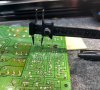
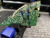
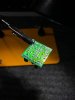
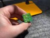
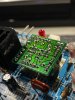
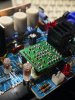
Rebuilding the daughter board which houses the differential input circuit was easy. I was careful to not heat stress the sensitive FETs, so a special lead heat sink tool was used.
The finished product turned out to be very nice. No more dry solder joints!

photo_2022-01-29_16-19-57.jpg photo_2022-01-29_16-19-59.jpg photo_2022-01-29_16-20-01.jpg photo_2022-01-29_16-20-03.jpg
 
Last edited:
Left amplifier section cont’d:

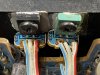
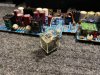
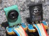
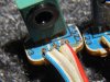
This small pair of transistors was mounted to the main heatsink remotely via a small wire loom and a tiny PCB. Kyocera decided to coat the wires with the famous corrosive glue for seemingly no reason. As standard, the corrosion worked its way through the entire wire loom, so it had to be replaced. Small details like this are what will ensure this amplifiers working condition for years to come. If this hidden corrosion were to have gone unchecked, I'm sure it would have caused serious issues. The devil is in the details...

photo_2022-01-29_16-25-34.jpg photo_2022-01-29_16-25-21.jpg photo_2022-01-29_16-25-24.jpg photo_2022-01-29_16-25-23.jpg photo_2022-01-29_16-26-09.jpg photo_2022-01-29_16-25-25.jpg photo_2022-01-29_16-25-26.jpg photo_2022-01-29_16-25-27.jpg

Like I mentioned earlier in this thread, all of the thermal compound in this amplifier was as dry as a bone. I remounted all of the TO-220's onto new silicone thermal interfaces on this amplifier module as well.

photo_2022-01-29_17-07-29.jpg photo_2022-01-29_17-07-35.jpg
 
Last edited:
Back
Top Bottom