• The move to the new server is done. There are some software and database maintenance updates in process. This has us passing the hat around to help out. We appreciate any donations. Seriously, even a dollar helps. The payment page may be found here - https://www.audiokarma.org/support.html

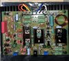
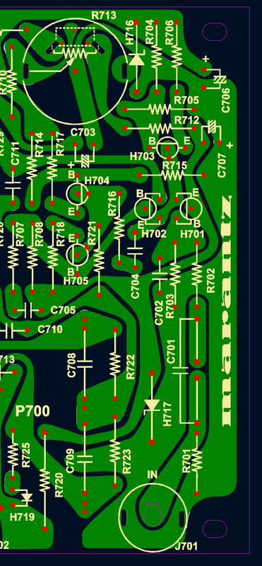
Marantz 2325 P700 exact PCB dimensions needed.

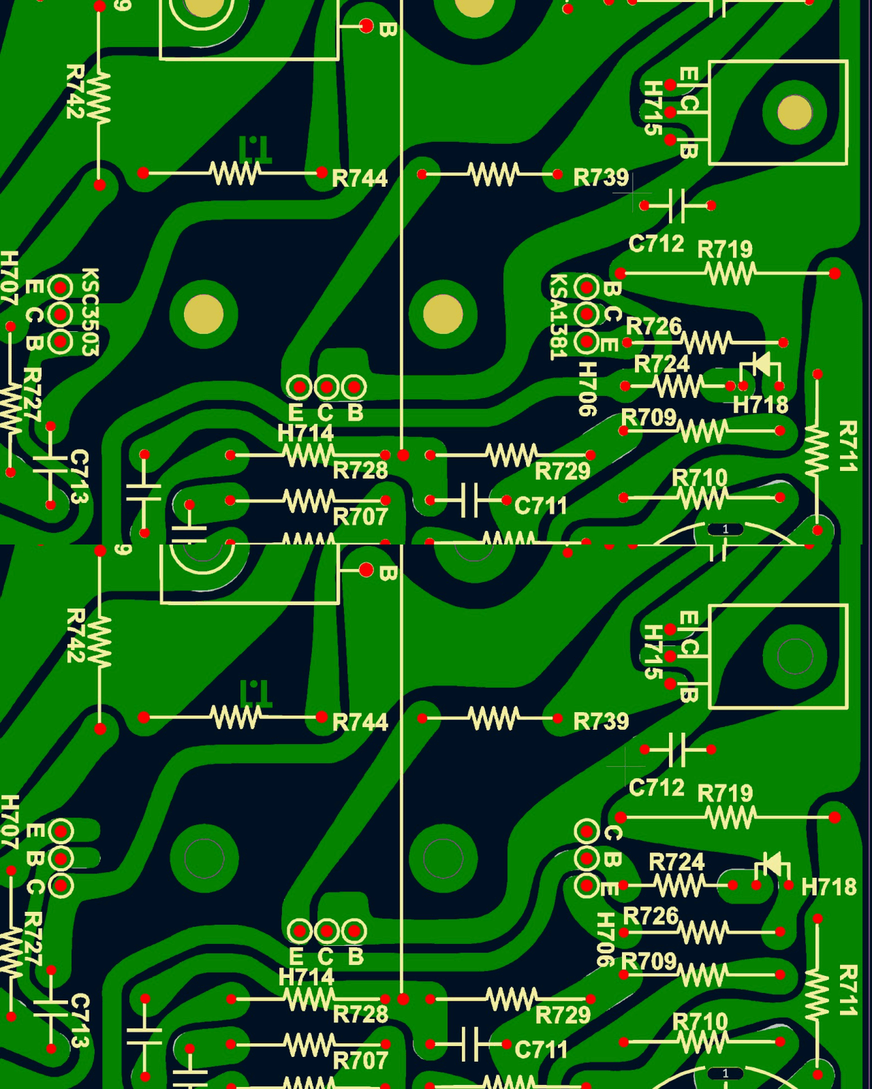
A year later, I made a revision of this PCB, to fit currently available transistors H706, H707 - KSA1381, KSC3503. Here is the picture with animated before/after view:
2325-p700-revision.gif


2325_mod.jpg
 
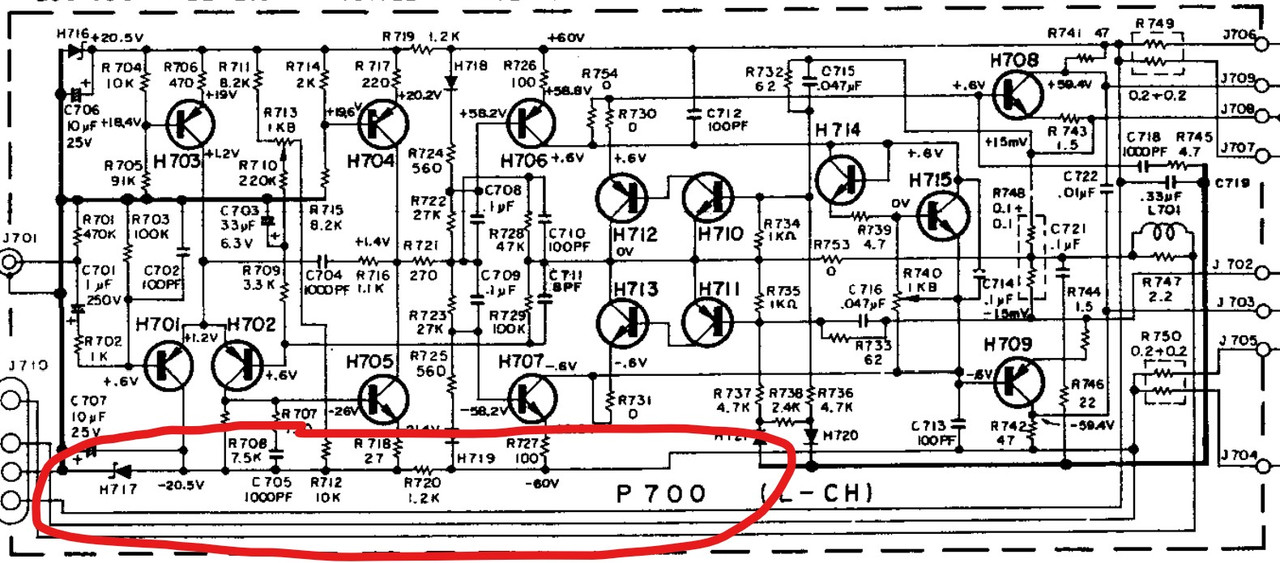
I was making a clean copy of the 2325's P700 schematic (attached PDF for downloading) and I noticed that there is no connection wire between these two parts of the GND in the original schematic:
2325-GND3.jpg

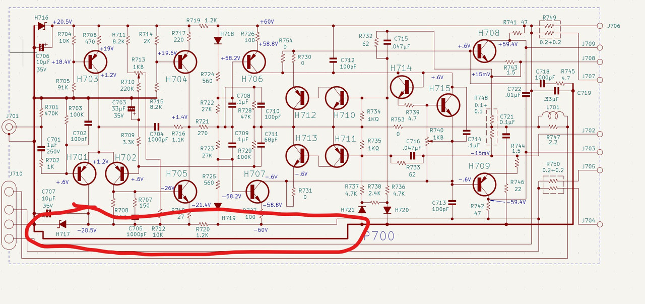
So I added one:
2325-GND2.jpg

Also noticed, that for this part of the P700 PCB, there will be no GND connection if the input signal J701 jack is not connected:

2325-GND.jpg
 

Attachments

I was making a clean copy of the 2325's P700 schematic (attached PDF for downloading) and I noticed that there is no connection wire between these two parts of the GND in the original schematic:
2325-GND3.jpg

So I added one:
2325-GND2.jpg

Also noticed, that for this part of the P700 PCB, there will be no GND connection if the input signal J701 jack is not connected:
2325-GND.jpg
Nice as long as it doesn't create a "ground loop". Real world testing would be a wise thing to do just to be sure.
 
Nice as long as it doesn't create a "ground loop". Real world testing would be a wise thing to do just to be sure.
Sorry, I didn't understand what is the problem with the "ground loop" in this case, maybe I didn't explain the discrepancy on the schematic properly... On the original schematic is obviously missing the connection between the two parts of the common ground - this connection is present on the PCB, so no problem there. The problem is only on the schematic. The ground on the showed part of the PCB is only connected to the "rest" of the GND via the J701 jack's wire, so if it is not connected with the signal plug, there would be no GND on that part of the PCB. I mentioned it just to be considered if someone is making measurements or tests and forgot to connect it.
 
Sorry, I didn't understand what is the problem with the "ground loop" in this case, maybe I didn't explain the discrepancy on the schematic properly... On the original schematic is obviously missing the connection between the two parts of the common ground - this connection is present on the PCB, so no problem there. The problem is only on the schematic. The ground on the showed part of the PCB is only connected to the "rest" of the GND via the J701 jack's wire, so if it is not connected with the signal plug, there would be no GND on that part of the PCB. I mentioned it just to be considered if someone is making measurements or tests and forgot to connect it.
Ahhh, OK. Carry on... :D
 
Back
Top Bottom