• The move to the new server is done. There are some software and database maintenance updates in process. This has us passing the hat around to help out. We appreciate any donations. Seriously, even a dollar helps. The payment page may be found here - https://www.audiokarma.org/support.html

Mixed up phono1 with aux1 after having disconnected everything

Birima

Member
Dear members,
I have worked for days and nights to open my Marantz 2385, cleaning all pots, selectors, and push buttons, rewiring the tuner cord, and fixing some bulbs including the one from the dial pointer and stereo indicator. I am a total newbie so it has probably taken me longer than average. Tonight I was able to close the beast and finally wanted to enjoy it. Despite the facts that I have taken many pictures when disconnecting a.o. the tone board, I must have made an error when putting them back. The problem is now that Phono1 and Aux1 have been switched! Apart from that, everything works and sounds much better. I do not know how to read diagrams so my question is if someone could direct to the right place (connector) in order to correct the problem.

It is important to mention that I have 2 AUX and 2 Phono inputs, however, the official Marantz diagram only shows 1 AUX. Thanks!

(English is not my native language)
 
Last edited:
Register to hide this ad
IMG_3780.JPEG Have narrowed down the problem to the input selector:

Phono1 = Phono2
Phono2 = Aux1
Aux1 = Phono1
Aux2 = Aux2

Maybe the first waver in line has shifted one position hence the connectors were connected correctly after all? Going to open it again and will update. Any input is welcome.
 
Some input selectors have been known to slip and not engage correctly. Check to see if the shaft has movement forward/backward that could cause a misalignment of the wiper on one of the wafers.
 
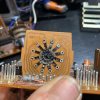
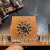
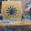
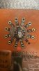
Thought I had found it by taking the shaft out, turning it around and the first waver has now another diametral position that even looks like an example on the forum. Did put back everything and the result is very disappointing: now only the radio works and only the right channel! everything else is dead, See picture one when I had still music albeit with mixed up aux and phono, and picture two as how it is now. Problem is that I do not really have an understanding of these selectors, maybe the two behind the first one also had to change position.
thumbnail_IMG_3822.jpg thumbnail_IMG_3824.jpg
 
OK. Let's try to get these aligned correctly.
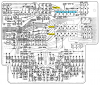
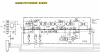
First, here is a layout of the board (might be slightly different for European version).
  • There are 3 selector wafers: S401-1, S401-2, & S401-3
  • Each of the 3 wafers has a Front (F) and Rear (R) side
  • Your picture above is showing S401-1F (shown in blue on the board layout)
  • Does this board mount with the component side down? If so, then the schematic may show the switches rotated 180 degrees. You can verify by checking the schematic against your board J408 and J410 connector pin layouts.
upload_2023-1-9_23-16-42.png
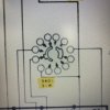
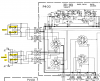
Here is the board schematic showing the 3 wafers and both front and back sides.
  • I have circled (in blue) the selector wafer that looks like your photo (S401-1F).
  • Take a good look at the position of the semi-circular conductor near the center.
  • If I remember right, the schematic shows the switch position for the left most position of the selector knob (AM).
upload_2023-1-9_23-35-8.png

Here is what you need to do:
  1. Rotate the wafer S401-1F so it matches the diagram above (this should be the AM position)
  2. The rear of S401-1R should match the diagram just above the blue circled one. (If you look at the back side of the switch wafer it might be a mirror image)
  3. Now leave this first wafer alone.
  4. Next, rotate the 2nd wafer to match the diagram of S401-2F (shown on the top left of the figure)
  5. The rear of the switch should look like S401-2R (or mirror image).
  6. Leave this wafer alone
  7. Last, rotate the 3rd wafer to match the diagram of S401-3F (shown on the bottom left of the figure), without turning the first two wafers.
  8. The rear of the switch should look like S401-3R (or mirror image)
  9. Now that you have aligned all three wafers, the rectangular slots should all be in-line as you look through the center hole.
  10. If they don't line up, please recheck the schematic.
  11. Next, insert the shaft and selector knob into the rectangular hole while keeping the knob pointer mark at the AM position.
  12. Secure the shaft and try it out.
Hopefully, this will solve your problem with the selector. Please let me know how it goes. Post pictures if you have a problem.
 
Last edited:
First of all, thank you so much for your kindness to put this all here! Just some thoughts I have: what if the first waver position (when almost everything was playing) was good after all and the problem is caused by malpositioning one or two of the Molex connectors? Is it possible to cause damage when the selector is out of sync (why did the left channel stop?) It's too bad I cannot test positions with the boards out since putting everything back together is such an arduous task. Okay, that being said, I will try to understand what you wrote now and keep posting
 
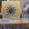
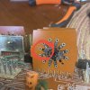
I just finished lining up according to the layout in the schema. Shown in picture one is S401-1F, in picture two is S401-3R, in picture three S401-3R as depicted in the schema (did S401-2 as well but is difficult to take a picture since it is in the middle). As one can see, S401-3R in real doesn't exactly line up with the example in the schema but it is the only way to have the rectangular hole leveled horizontally. Maybe the difference is that I have Aux1 and Aux2.
thumbnail_IMG_3834.jpg thumbnail_IMG_3837.jpg thumbnail_IMG_3836.jpg
 
Last edited:
I now discover that there are two Molex with the same wire color combination pink, black, white, but do have a different color of socks. One comes from the balance that ceased working last night (only the right channel). I most likely have mixed them up!
 
Your switch wafer photo above is not correct. See the diagram below.
Since your photo is the back side of the wafter you need to reverse the image to match the schematic diagram.
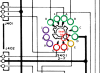
I tried to match colors and (arbitrary) letter labels between your photo and the schematic for reference.
You need to rotate the small tab in the white circle on the left photo to position it next to the orange contact I have labeled "I".
It is exactly 180 degrees from where it should be. Just rotate it 180 degrees and it should be OK.
Do you see now?

upload_2023-1-10_7-51-30.png

Here is the alignment for the first wafer, S401-1F (front side).
upload_2023-1-10_8-17-23.png
After you do this, the center slotted holes should match up and it looks like almost horizontal.

Do the same for the 2nd wafter then insert the rod into the center slot. (Front side)
All of the slots should line up now.
upload_2023-1-10_8-44-32.png

This should do the trick.
Let me know how it goes.
 
Last edited:
As for your cables... see if the cables have J numbers on them and match them up to the schematic and board connectors.
Take a photo of the cables if you can't figure it out.

upload_2023-1-10_8-29-4.png
 
Good heavens, I was already in the process of closing it up! Thank you very much again. As for the front waver, the picture you used is not my last adjustment or I don't understand it (see the last adjustment below). Is it correct that the rectangular hole should be positioned horizontally (thus all of them)?


thumbnail_IMG_3834.jpg
 
Last edited:
I think it is close, maybe rotate it just a little counterclockwise. Maybe so the slot is horizontal.
Now align the 2nd and 3rd wafers and it should be good.
upload_2023-1-10_11-44-26.png
 
I hope I got it right now, for S401-1, I have used the front, S401-2 and S401-3, I have used the backside because of a better view. The small tabs are in the red circles, in the second picture you can just see it:
thumbnail_IMG_3842.jpg thumbnail_IMG_3844.jpg
 
It looks like it is good now. I assume you did the same for the 2nd wafer. Did you check the wiring connectors to the board also? You thought you found the error.

Also, while you have it apart, clean the wafer contacts with isopropyl alcohol or Deoxit contact cleaner spray.
 
Last edited:
Hi Dankik, I have good and bad news:

Radio in reverse mode only right channel, in stereo mode only left channel, L+R both channels, L both channels, R no channel. When using the selector the radio needle bulb keeps burning, also in i.e. aux1, aux2 etcetera.

Aux1 in reverse mode only right channel, in stereo mode only right channel, L+ R only right channel, L only right channel, R, right channel.

Aux2 in reverse mode only right channel, in stereo mode only left channel, L+R both channels, L both channels, R no channel.

Tape1 nothing nowhere

Tape 2 seems to work and both channels!

The cables do not have position marks written on them but I have made plenty pictures during demontage. Kindly share your thoughts.

Regards
 
Last edited:
Maybe it has to do with having an Aux 2 input not shown in the schema. I have opened the device very rapidly this time by removing the face plate and the plate after that one. Took the selector out again.
 
Last edited:
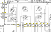
The schematic that I used is for the European 2285 (see below). I assume this is what you have. The Marantz SM schematic is slightly different (I think).
upload_2023-1-10_17-0-22.png
It has two AUX inputs (and 2 Phono inputs):
upload_2023-1-10_17-1-51.png
And, 2 Tape In/Out on the back with one on the front also.
upload_2023-1-10_17-3-36.png

It will take me a while, but I can follow the wires going into the P400 board and you can make sure it is coming from the right places. Am I correct in assuming that the cables do not have any markings with connector J numbers/
If you can post a photo of the board with the wires connected, it may help me to understand what you did.
In terms of burning out a lamp, it could be that one of your connections is incorrect.
 
The panel lamps (PY00) connect to the P400 board through the connectors on the bottom of the schematic.
You could be blowing lamps if you have an incorrect connection to the PY00.
upload_2023-1-10_17-20-46.png
 
Back
Top Bottom