• The move to the new server is done. There are some software and database maintenance updates in process. This has us passing the hat around to help out. We appreciate any donations. Seriously, even a dollar helps. The payment page may be found here - https://www.audiokarma.org/support.html

Need Bias Current Help with Sansui AU-20000 (0 mv)

Utk

New Member
Hi everyone,

I'm experiencing an issue with my Sansui AU-20000 amplifier. When I set the low pass filter on the front panel, the amp goes into protection mode, and a loud pop is heard from the speakers.

The amp is quite old, so I decided to recap all the boards and change some transistors, following this thread:
Another AU-20000 Restoration (post #6)
Another Post with a similar issue

After recapping, the ±65 Volts became intermittent. I noticed a broken trace on the F-2511 board and patched it. Now, all the voltage rails look good.

I was able to set the DC offset to 0mV ± 1.5mV. However, I cannot set the bias current according to the manual's specification of 35mV between pins 2 and 4. It sits at 0.05mV and doesn't move at all, regardless of the VR02 position on the F-2507 board.

There is no extra power draw, and it consumes about 40-45 watts idle (powered via a Voltage Controlled AC power supply).

I tried looking through other posts but couldn’t find a satisfying answer.

Eventually, I removed the F-2497 assembly (heatsink blocks) and noticed that TR01 (2SC1364) is missing. It seems it was never there, as the vias are super clean, indicating it hasn't been removed. The amp used to work without it, and in the thread linked above, it appears TR01 is not on that board either.

Has anyone encountered this issue before? Any advice on how to resolve it or debug this problem would be greatly appreciated.

Thanks a lot!
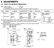

Screenshot 2024-07-01 at 7.43.08 PM.png
 
Last edited:
Register to hide this ad
The bias transistor (TR01) was originally located on F-2497. In later production it was relocated to the F-2507 driver board where it is identified as TR12.

If the bias setting issue is on both channels then likely there is a problem with the power supply.
 
The bias transistor (TR01) was originally located on F-2497. In later production it was relocated to the F-2507 driver board where it is identified as TR12.

If the bias setting issue is on both channels then likely there is a problem with the power supply.
Thank you, I’ll look at F-2508 first then.
 
Thank you, I’ll look at F-2508 first then.
You should look for a faulty trimmer, Bias transistor, dry joints, lifted track, faulty resistors (out of spec), and faults with any of the pre-driver and driver transistors, and finally the output transistors and their emitter resistors.

You won't be able to tell if they are faulty just by looking at them, you will almost certainly need to remove components to test them properly. Experienced tech's often use a multimeter on ohms range to check semiconductor junctions and resistors outside of the unit.
 
Last edited:
Verify dc voltages on F-2511 as a starting point. But before that, where are you up to with the main heatsink assemblies? F-2497 may need some attention before being refitted.
 
So I started with the schematic and am trying to test everything one by one.

F-2511’s +-68V & +-85V rails look ok. I am not sure what the circuit driven via Fuse F04 is doing in 2511. (I need to make sure this is working ok, looks like the output V, W tied to speaker terminals.

I just went through F-2508 and verified that everything looks good. It’s putting out +- 70 instead of +-65.

+-35 looks good.


Next I am going to look at F-2507 & F-2497

I am suspicious that I screwed up something on F-2507.


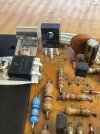
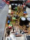
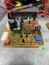
Here is a photo of my current progress:
IMG_0263.jpeg
 
Verify dc voltages on F-2511 as a starting point. But before that, where are you up to with the main heatsink assemblies? F-2497 may need some attention before being refitted.
haven't opened F-2497 yet. Will look at it now. I want to verify F-2507's bias circuitry first. Because taking apart 2497 seems like a task given how the output transistors are placed. Thanks for the help, I'll keep you updated.
 
Ok, hold on there. We'll go one step at a time. Are the main heat sinks installed in the amp?

If not, refit the heatsinks assemblies. Make sure they are secure and pay close attention to the wiring, especially the connections to F-2512.
 
Last edited:
The voltages on F-2511 look okay but suggest you're not using a dim bulb tester. A DBT would provide some current limiting protection and would be advisable when testing,

Where did you take +/-68Vdc measurements from on F-2511? You should see voltage on pins 29 and 30 as well as the connectors 7 and 8.

Pins 29/30 connect to the driver transistors. Connectors 7 /8 connect to the output transistors.
 
It's not easy to read your schematic notations, but it looks like you have voltage at the right places: +/-65V regulated and +/-68V unregulated for the driver boards, +/-68V for the output transistors. (Noted that +/-70V on the output of F-2508 is abnormally high.)

With the power off, make a quick resistance check across pins 2 and 4, the bias current test points. You should see a reading of around 1.2Ω, being the approx value of the two emitter resistors plus lead resistance.

If that's okay then please post photos of at least one of the driver boards, both component and conductor side, with a list of the component changes you've made.
 
You could also check the voltage at 27 and 28 on each of the F-2497 boards. Normally you would expect see approximately +/-500mVdc output from the driver transistors, however it might be closer to zero if you've made an error on the driver boards.
 
1. Pin 2-4 read about 1.2~1.3 Ohms

2. Noted High Voltage on output of F-2508
Could this be because I tested it while I took out the Driver boards. (I did so because I wanted to just test the F-2508 and didn’t want the F-2507 to pull the voltage down. Maybe it’s high coz F-2507 is not plugged in ?)

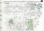
3. I attached a high res PDF

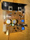
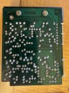
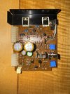
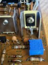
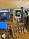
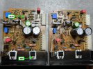
4. Photos F-2507
- Changed all Caps except ceramic
- All Diodes
- All Transistors except TR12 (bias transistor)
 

Attachments

  • IMG_9139.jpeg
    IMG_9139.jpeg
    141.3 KB · Views: 19
  • IMG_9138.jpeg
    IMG_9138.jpeg
    118.3 KB · Views: 19
  • IMG_9137.jpeg
    IMG_9137.jpeg
    146.6 KB · Views: 17
  • IMG_9136.jpeg
    IMG_9136.jpeg
    142.3 KB · Views: 18
  • sansui_au-20000_sm 2-compressed.pdf
    sansui_au-20000_sm 2-compressed.pdf
    550.4 KB · Views: 9
Last edited:
Swapped TR04/5 with kSA1220 / KSC2690
I know the original 2SA818/2SC1628 has the base bolted on to the aluminum bracket.

Could that cause any issue ?

IMG_9142.jpegIMG_9141.jpegIMG_9140.jpeg
 
Hi-res of schematic is much better to read, thanks.

I can't immediately see anything wrong on the boards. TR04 and TR05 do not require an insulator and would be better off without it.

See post #13 and let me know what you find.
 
60mV is not enough to turn on the output transistors.

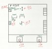
Lets check the power supply directly from the board before looking more closely at components. Working on one driver board alone, install it in the left channel slot, being the one closest to the main heatsink. Leave the other board aside to give better access to the components. (The images are from another AK member's amp, annotations are mine.)

F-2507 +:-63V.jpgIMG_1204.jpgIMG_1201-1.jpg
 
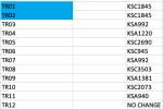
Here is my swap list:

Screenshot 2024-07-05 at 9.07.15 PM.png

I am now doing what you recommended in Post #18. Again thanks a lot, this has been very helpful.
 
60mV is not enough to turn on the output transistors.

Lets check the power supply directly from the board before looking more closely at components. Working on one driver board alone, install it in the left channel slot, being the one closest to the main heatsink. Leave the other board aside to give better access to the components. (The images are from another AK member's amp, annotations are mine.)

View attachment 3244093View attachment 3244094View attachment 3244096
Looks ok with both driver boards plugged in one at a time to test.

IMG_88F49C4877B1-1.jpeg
 
Back
Top Bottom