• The move to the new server is done. There are some software and database maintenance updates in process. This has us passing the hat around to help out. We appreciate any donations. Seriously, even a dollar helps. The payment page may be found here - https://www.audiokarma.org/support.html

One giant leap for a man, one small step for mankind - learning how to solder

Update:
Over the past month I've been playing with various cheap DIY kits, like an LED clock, a pocket calculator, an hourglass (different from the one above, and this time I didn't mess anything up), a game console, a pocket FM radio (no video of that, sorry), and a few other things.
I am now confident I can tackle any THT soldering job without breaking a sweat. I get perfect joints every time. As for desoldering... I do occasionally encounter a stubborn joint, but in the end I manage to defeat it one way or the other. While as recently as two months ago I dreaded soldering and was completely useless at it, now I can do THT with my eyes closed.
So, I thought it was time to move on to SMD.

The first technique I had to learn, and quite early on at that, was drag soldering, because I needed it for the hourglass I talked about above. This was pretty easy. Somehow I got the hang of it immediately and never had an issue. At first I used to tack two corners of the chip and then solder the rest, but now I can skip that step. I can easily hold the chip in place with one hand, with a pair of tweezers, while loading the soldering tip and then dragging it across the legs of the chip with the other.

OK, so SMD chips are easy, but how about those tiny resistors or capacitors that you can barely see with a magnifier, let alone with the naked eye?
First, I tried to apply the same soldering technique that I used with THT. This kind of worked, to an extent, but resulted in big blobs of solder:
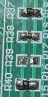
IMG_2473_1.jpeg

Horrible. Yuck!

The problem, I realized, was that the 0.8mm solder that worked so beautifully with THT was much too thick for SMD. No matter how gently I tried to touch the component with the solder wire, and how quickly I tried to withdraw it, I just could not get that teensy-weensy amount of solder that I needed.
Obviously, SMD required thinner solder wire. So I went ahead and got some 0.25mm.
Now we're talking! No more blobs. Now I can feed the wire slowly and controllably without drowning the component in solder.
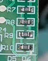
IMG_2474.jpeg

It looks much better. Not quite perfect, mind you, but definitely presentable.
But the trouble is, it's extremely fiddly, takes a lot of time, and doesn't always turn out that nice-looking. It's a bit hit and miss. Maybe with more practice it would become more hit than miss, but deep inside I wasn't entirely satisfied. I can do it if I have to, but I would be happier if I could find a better method.

The more I read about SMD, and the more videos I watched, the more convinced I became that in order to master SMD one needs a hot air station. Sure, you can do without if you really have to, but it makes life much easier (or so it seemed). So, I got myself a relatively inexpensive, but seemingly well regarded, hot air station and got to work.

A tiny bit of solder paste on each pad, then carefully placed and aligned the components, then hit them with the hot air. And here's the result:
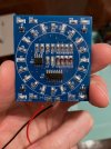
IMG_2470.jpeg

IMG_2471.jpeg

IMG_2472.jpeg

I did them in batches of three or four, covering the already done neighbouring components in aluminum tape to protect them from the heat and keep them from melting again.

I made sure that the values printed on the resistors were always aligned with the labels on the board. And when this was not possible, at least I made them face the same way. I do this with THT, too, I mean I place all resistors so that their colour bands have the same orientation. You can tell I suffer from OCD, can't you? :biggrin:

Of course, nice-looking joints mean nothing if the device does not work. But fortunately it does:

 
Last edited:
The only thing that puzzles me is that the solder takes on a matte appearance after it cools down, as if it were lead-free, although it isn't. It's actually Sn63%/Pb37%. :dunno:
 
The only thing that puzzles me is that the solder takes on a matte appearance after it cools down, as if it were lead-free, although it isn't. It's actually Sn63%/Pb37%. :dunno:

Probably a little residue from the flux. Does it shine up if you take a Q-tip and some IPA to the joint?

Don't worry too much about shininess. One of the first things we were taught in solder training was that a shiny joint is not always a good one nor is a dull joint always a bad one. The single most important thing to look for is the whetting. The solder needs to flow smoothly to a feathered edge with no undercutting.
 
Good for you :thumbsup:an your intense wanting to master this delicate procedure that requires both dexterity, proper tools and patience.

It is indeed a separate craft of its own when it comes to "fixes".

Q
 
Probably a little residue from the flux. Does it shine up if you take a Q-tip and some IPA to the joint?

Don't worry too much about shininess. One of the first things we were taught in solder training was that a shiny joint is not always a good one nor is a dull joint always a bad one. The single most important thing to look for is the whetting. The solder needs to flow smoothly to a feathered edge with no undercutting.
No, it doesn't seem to be residue. It won't wash away with IPA. But I'm not worried. I'm sure the joints are fine. It's just that I used to think that shiny equals leaded, and dull equals lead-free (assuming good joints in both cases, that is). But maybe it's not so clear-cut. Maybe most leaded solders dry shiny, but not all.

Good for you :thumbsup:an your intense wanting to master this delicate procedure that requires both dexterity, proper tools and patience.
It is indeed a separate craft of its own when it comes to "fixes".

Q
Thank you.
When I started on this journey, all I wanted was to become less hopeless at something that so many people seemed to have no trouble with, and to make it seem less like a chore and more like a simple task that I could tackle without fear if I had to. I didn't think I'd discover a new hobby. But to my surprise, I find that I'm really enjoying it, and I want to go deeper and deeper into it. It is quickly turning into a hobby.
But of course, soldering is not an end in itself. Its whole purpose is to build or repair stuff. And I'm not yet qualified to do either. I've got an awful lot to learn on that front. I will work on that, too.
 
Last edited:
Nice work there, Vlad.
Liquid flux and variable tip temperature are your friends. Cleanliness, tip contact, and dwell as well.
Soldering is so similar to welding. The metals and temperatures and colors are different, but the concept of flowing liquid metal together remains and has always fascinated me.

Hmph!
Try TIG welding sometime—but only if you can walk and chew gum at the same time. Even then, it's an order of magnitude skillwise.
-k
 
Update:
Over the past two months I concentrated on getting acquainted with basic electronics, reading a lot, building small circuits on the breadboard, trying to understand how they work and why, how to read a schematic, how to write one, stuff like that.
I have played around with transistors, MOSFETs, a few simple chips like 555, 4017 or 4026, learned how to use a seven-digit display in a circuit and how to display a digit of my choice on it, and I have also got an Arduino and learned how to use it. It's been a long time since I last wrote a line in C, but apparently C is like riding a bike. It came back to me in no time. :biggrin:

Now that I've assembled quite a few toys of the sort presented above, I thought the next logical step would be to try and figure out how they work, draw a schematic for each one, understand the exact purpose of each component in the circuit (hence the other thread), and then maybe reproduce it, or create a variation of it, on the breadboard first, and then maybe on perfboard.

One of the simplest of those kits had a bunch of red and blue LEDs. Theoretically it was supposed to alternate blue and red like a police car, but actually wasn't doing exactly that. It had a strange pattern - blink red three times, then blink blue three times, with the time between colours much shorter than the time between two blinks of the same colour.
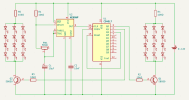
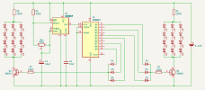
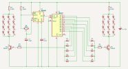
I examined the PCB and came up with this schematic:

Orig.png

The idea is simple, and the schematic explains the blinking pattern. The 4017 chip counts from 0 to 9 whenever it receives a signal on its clock pin from the 555 astable oscillator. The pins for 0, 2, 4 are connected to one group of LEDs, and the pins for 5, 7, 9 to the other group. So it counts red-pause-red-pause-red-blue-pause-blue-pause-blue-red-pause-red-pause-red... etc. The diodes are necessary to prevent the signal from the active pin going back to the inactive pins. All clear.

So I thought, can I improve it? Can I make it blink alternately, red-blue-red-blue, with a constant frequency and no strange pauses between red and blue? At first glance, it should be pretty simple with minimal modifications. Just wire all the pins for odd numbers to one transistor, and all the pins for even numbers to the other. Problem solved.

I modified the schematic accordingly:

768969714_27434066969623058_1104486997065006009_n.jpg

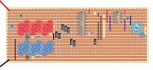
and then, based on it, I created a draft of the layout using a free app called DIY Layout Creator:

769313194_27434157059614049_4578643939848513691_n.jpg
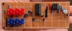
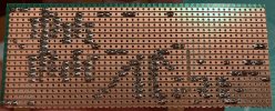
Once the layout was complete, the actual build was fairly quick and easy. And here's the result:

766320985_27434065556289866_2806279228805482837_n.jpg
768949740_27434435452919543_4994477452539431227_n.jpg

And it works!


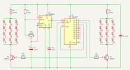
It was only after building and testing it that I realized something. I had made it too complicated. Instead of letting the 4017 count from zero to nine and using all the odd and even outputs, I could make it count only from zero to one. Connect the pin for 0 to one transistor, the pin for 1 to the other transistor, then connect the pin for 2 to the reset pin. This way, after 1 it will go back to 0. And then I wouldn't need any diodes, since no two output pins would share a connection anymore.

Like this:

Final.png

I desoldered eight of the diodes, connected a wire between pins 4 and 15, and it worked perfectly, so the idea is sound.

One thing gave me a lot of headache when I first built the original. The red LEDs worked fine, but the blue ones didn't. I spent the best part of an hour trying to debug it, measuring each and every spot with a multimeter, measuring continuity and voltages, and everything was absolutely perfect. I even probed the transistor for the blue LEDs with the oscilloscope and proved that the base received a voltage at the right moments, and that the collector-emitter connection did close. Everything was perfect. All LEDs were functional; I had tested them all with the multimeter, and they all lit up. So what in the name of all that's holly was happening?
After a lot of head scratching, I got an idea. You see, the LEDs were connected in three parallel groups, each group having four LEDs in series. In series the voltage divides equally among them. And I remembered that blue LEDs have a much higher forward voltage than other colours. The red ones had approximately 1.7V. The blue ones I couldn't measure, because they exceeded the threshold of my multimeter, but I expect them to be somewhere between 2.7V and 3V. So, even though it said "9-12V" on the PCB, it actually couldn't work with 9V.
I increased the voltage, and voilà! It worked perfectly. :smoke:
I spent an hour chasing an inexistent fault. :rflmao:
 
Last edited:
After having built a few small circuits on the breadboard, I thought I'd try and see how I could go about making something more permanent. Not that those particular circuits really deserved being made permanent, mind you, but just as a learning experience.

First, I tried a plain perfboard, the kind with unconnected holes.
Pros: looks good, feels good and sturdy, tinned pads make soldering a breeze, overall closest in look and feel to a proper PCB.
Cons: an absolute nightmare to connect the components to each other, and downright impossible to do it in a beautiful, elegant manner.
I tried making the simplest circuit I could come up with - a 555 timer in astable mode that causes an LED to blink once per second. Figuring out how to make the connections was a nightmare, and actually making them was even worse. In the end I did it, because I was really determined to make it work, but I hated it. It worked, but it looked ugly and it took twice as much time and ten times as much effort as it should have.

So then I moved on to striboards, like the one pictured above.
Pros: pre-built strips make it easy to connect the components to each other, by grouping them into nets and assigning a strip to each net.
Cons: looks cheap, feels flimsy, and the solder tends to spread a bit towards the neighbouring holes, taking on a rectangular rather than round shape, which makes it look somewhat amateurish. Also, it's less space efficient, though this can be minimized with a bit of careful thinking, by breaking the strips at specific spots and reusing the resulting segments, like I did above.
Boy, what a difference! Getting from the schematic to the built circuit is incomparably easier and faster than with the plain perfboard. I'm using a free app to design the layout based on the schematic, after which the actual build is a piece of cake. If you're interested and have a half hour to spare, here's a nice tutorial for that app.
As an aside, the same app is great for making layouts for the breadboard, too (tutorial for that here), so I heartily recommend it even if you're not using stripboards.

Now I'm trying to go to the next level.
Having learned how to make schematics in KiCAD, I thought I'd give PCB design a try. At first it looked overwhelming. Scary even. I thought, there's no way I'll ever be able to do this. All the components mashed into one another, with a jumble of ghost connections between them (I would later on find out they're called 'air wires')... How do I even begin to sort out this mess? So I gave up. Then tried again, then immediately gave up again. But two days ago I was determined to do it, come what may. I started, of course, with the simplest circuit, the good old astable 555 with an LED. And after several attempts it looked like I had finally got something that might be usable. I sent the Gerber files to a local company that specializes in custom PCB manufacturing, and even though it was a Saturday afternoon they responded instantly and were kind enough to give me a few hints to improve them.
Having done that and learned that PCB design isn't really as scary as it first seemed, I gathered up the courage to make one for the above red-blue blinker. This time I paid more attention not just to the functional side, but also to the layout itself, trying my best to make it look as elegant and professional as possible. After ensuring that the Design Rules Checker found no errors and warnings whatsoever, I sent them the new files, and they confirmed they were entirely correct and can be manufactured.
So, fingers crossed. I should have the PCBs in a few days. I will keep you updated. I'm not showing you the design yet. I want to show you the real thing, if it turns out as expected. :)
 
Last edited:
WOW you're determined !!!

Awesome! Too many people give up and don't have faith in themselves , but you are an inspiration to many who will read this and hopefully your enthusiasm will be infectious .

Athanasios
Thank you. ❤️

At first I didn'think I'd discover a new hobby, but the deeper I go into it, the more it turns into one. And also, the more I realize how little I know and how much there's still to learn. But at least it doesn't seem so scary anymore.
Having had a technical education and a good understanding of electricity, and of physics in general, does help a lot. When I search for information on the subject, I am fortunate enough to understand it. But still, it's a big, big field, which is completely new to me, and so far I've barely scratched the surface.

On a different note, I didn't forget I promised to keep you updated on my first attempt at PCB design. But I haven't received it yet. It's taking a little longer than I first thought. I thought it would be as easy as uploading the Gerber files into a big machine, pushing a button, then having the PCB produced thirty minutes later and shipped the next day. But apparently it's not that simple. I read a bit about the process, and it seems there are many steps, some of which are quasi-manual, and it can sometimes take as much as two weeks. :oops:
 
Last edited:
I received the PCB today.
Here's the schematic again:

Screenshot 2026-08-25 at 19.31.09.png

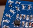
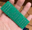
And here's how it turned out:

IMG_2658.jpeg

Now that I see this picture, I notice a few things that trigger my OCD, which I missed in the design. R4 and R5 should have had the labels placed the same - either both above, or both below the resistors. And R1 could have been vertically aligned with R2 and R3.
Next time I'll be more careful. But as a first attempt I'm really pleased with it.

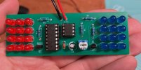
The end result:

IMG_2661.jpeg
IMG_2662.jpeg

And... it works! :biggrin: :cool:


I can't believe I made this myself. If someone had told me a few months ago that I will some day make something like this from scratch, not just build it, but make it, all the way from design to the real thing, I'd have thought they were mad.
In all fairness, the design isn't entirely mine. I reverse-engineered someone else's creation. But at least I managed to understand it and to improve it, which until very recently would have been unthinkable.

Sure, it's a useless toy. Nothing impressive. But as I said, a small step for mankind can sometimes be a giant leap for a man... :)
 
Last edited:
Very impressive! You've certainly jumped in with both feet - great progress.

Don't feel bad about zapping your earlier project with the sneaky 9 V power supply. I've done far worse. I'm used to my old-school HP power supplies, all of which are clearly marked with their output ranges either in text on the top part of their front panels or easily determined by the numbers on the analog meter. At work we have a fair number of G.W. Instek power supplies with digital displays, most of which are 0-30 V, and the markings on them indicating the output range are small and underneath the binding posts (I LITERALLY just discovered this while looking up pictures of them refreshing my memory for this post). Being below the binding posts, they aren't clearly visible if you're standing at the bench - what can easily be seen is the model number (GPC-3030D, for instance, is a dual variable 0-30 V, 0-3 A PS, with an additional fixed 5 V output). I was trying to use a little handheld Brother labelmaker, but didn't have batteries for it. No worries, I'll grab one of the GWInstek supplies and some clip leads and jury rig it - I needed to make ONE label. Sitting on the shelf was a GPR-30H10D - perfect. Grabbed and connected it. Turned it on and started increasing the voltage output. Weird - the decimal point must not be working. Went ahead and cranked it up to the 9.0 V the labelmaker wanted. Remember that I thought the decimal point was out. Somewhere along the way up to "9" V, the labelmaker went 'POP', and I got a whiff of Eau de Allen Bradley. It was at that moment I discovered that this wasn't a 0-30.0 V power supply with a bad decimal point, but instead was a 0-300 V, 1 A power supply. I'd put 90 V into the poor labelmaker. D'oh!!! RIP, little guy!!

The first thing I did when I got the replacement labelmaker was to print out one that said "300 V max out" or something along those lines and put it on the top edge of the faceplate of that power supply! That was a rather embarrassing incident.

-Pat
 
Back
Top Bottom