• The move to the new server is done. There are some software and database maintenance updates in process. This has us passing the hat around to help out. We appreciate any donations. Seriously, even a dollar helps. The payment page may be found here - https://www.audiokarma.org/support.html

Sansui AI-317 mk1 - Troubleshooting and Repair

Hi,

Well done re the TR604 replacement.

Re the relay not engaging after the turn on delay, this can be due to higher than normal DC offset being present. This can be due to a fault or adjustment having drifted. You can check the DC offset on each channel by measuring the DC voltage between one of the bias test points and ground (chassis). it doesn’t matter which bias test point you measure on each channel. You can attempt to adjust the offset voltage if it is more than a couple of hundred millivolts. If it measures high (positive or negative) it is likely that a component or several components have failed or have gone out of spec. In any case measure the DC offset by measuring the DC voltage on one of the bias test points on each channel and report back.

Cheers
John
 
if i measure between the two pins at each test point, i read 0V.

if i attach the negative lead to chassis and touch positive to either pin of the left channel i read 30.1V and if i do the same for the right channel i read 29.8V at each pin.
 
Ok, you have high DC offset on both channels. Are the links that connect the pre amp out to the main amp in fitted to the amp? If so then remove them and measure the bias test points to ground as per your second paragraph and report back

Also, with the power switched off, measure the resistance across R35, R36, R45 and R46 on the main amp board (These can be measured “in circuit”, no need to lift one end or remove to measure). These should measure close to 150 ohms each. They are fuse resistors and will likely measure higher.
 
With preamp/power amp jumper cables removed the bias test points to ground measure slightly higher - ~31V both channels.

Fusible resistors:
R35 - 153 ohms
R36 - 157 ohms
R45 - 154 ohms
R46 - 130 ohms

These measurements seem fine? R46 is a bit off but I'm assuming not enough to cause the problem we're seeing.

I'm going to re-measure all of the voltage test points on the power board now that I have more experience locating components on the board using the schematics and diagrams in the manual - I may have missed something.
 
Those fusible will need to be replaced at some time, but they aren’t contributing to the high DC offset on both channels. there are also fusibles on the tone control board F-2752, but these aren’t marked as fusible on the either the schematic or parts list. They are R17 and R18, and they are 68 ohm. They will also need to be replaced at some stage.
 
Good call out re: replacing fusible resistors at some point.

Ok, the plot thickens.

I measured 4 transistors (indicated as voltage test points on the schematic) that I had neglected to look at before:

TR02 E pin - expected 7.6v, actual: 18v
TR04 E pin - expected 7.6v, actual: 16v

TR01 E pin - expected 7.6v, actual: 18v
TR03 E pin - expected 7.6v, actual: 16v

It seems implausible to me that all transistors could be faulty with such perfect symmetry. Are there other components nearby that could affect the voltage like this (capacitors, resistors, diodes)? Or do these transistors really do look bad?

I will also re-measure all of the ~42v test points now that I can find things on the circuit board more easily - it's possible I made mistakes there.
 
If you have a DC ofset at the output stage, the feedback to the input differential pair will try to compensate and this may be the reason why you are getting these results.
To me the question is why both output stages have similar DC ofsets?. I assume that none of your output transistors is open or shorted. They are easy to check since they are on sockets.
In the same context, Have you verified that none of the emitter resistors are open?. R57, R59, R58 and R60 are the resistors I am thinking about, especially R59 and R60 which are on the transistor that is on the negative rail. My reasoning is that an open emitter resistor on the PNP ouput transistor will cause the output to get yanked up towards the positive rail, and this will in turn upset the input differential pair by virtue of the negative feedback. Another pair of emitter resistors to be checked are those on the drivers, R49, R51, R50 and R51. In my opinion it is worth checking the values of these resistances.
 
If you have a DC ofset at the output stage, the feedback to the input differential pair will try to compensate and this may be the reason why you are getting these results.
To me the question is why both output stages have similar DC ofsets?. I assume that none of your output transistors is open or shorted. They are easy to check since they are on sockets.
In the same context, Have you verified that none of the emitter resistors are open?. R57, R59, R58 and R60 are the resistors I am thinking about, especially R59 and R60 which are on the transistor that is on the negative rail. My reasoning is that an open emitter resistor on the PNP ouput transistor will cause the output to get yanked up towards the positive rail, and this will in turn upset the input differential pair by virtue of the negative feedback. Another pair of emitter resistors to be checked are those on the drivers, R49, R51, R50 and R51. In my opinion it is worth checking the values of these resistances.
Thanks @JoseHH - I will try out your suggestions and report back
 
Also, if the fuses on the secondary side of the transformer haven’t been checked for continuity (checked with a meter rather than a visual inspection) then please check them.
 
If you have a DC ofset at the output stage, the feedback to the input differential pair will try to compensate and this may be the reason why you are getting these results.
To me the question is why both output stages have similar DC ofsets?. I assume that none of your output transistors is open or shorted. They are easy to check since they are on sockets.
In the same context, Have you verified that none of the emitter resistors are open?. R57, R59, R58 and R60 are the resistors I am thinking about, especially R59 and R60 which are on the transistor that is on the negative rail. My reasoning is that an open emitter resistor on the PNP ouput transistor will cause the output to get yanked up towards the positive rail, and this will in turn upset the input differential pair by virtue of the negative feedback. Another pair of emitter resistors to be checked are those on the drivers, R49, R51, R50 and R51. In my opinion it is worth checking the values of these resistances.
I didn't remove the transistors as I don't have any thermal compound to put them back in (i will order some, eventually). The resistors R57-60 are under the heat sink so I tried to test those in-circuit. The resistors have continuity but that's about all I can say since they all measured 0 ohms, probably because I didn't desolder one leg to take the measurement.

I took these measurements of the output transistors with the unit powered off and my multimeter in diode check mode.
TR20
B->E 0.14
B->C 1.8
E->B 1.4
C->B 0.49
TR18
B->E 0.14
B->C 0.48
E->B 0.14
C->B 1.66
TR19
B->E 0.14
B->C 1.85
E->B 0.14
C->B 0.49
TR17
B->E 0.14
B->C 0.49
E->B 0.14
C->B 1.68

Nothing jumps out at me. But perhaps the way I took the measurements is not very useful.

I will try poking around with the unit turned on to see if i can find some weird voltages connected to these transistors.
 
Hi,

Whilst you are having a look at voltages on the main amp board, can you measure dc voltage either side of R05 and R17 to ground (left channel), and either side of R06 and R18 to ground (right channel).
 
I took these measurements of the output transistors with the unit powered off and my multimeter in diode check mode.
TR20
B->E 0.14
B->C 1.8
E->B 1.4
C->B 0.49
TR18
B->E 0.14
B->C 0.48
E->B 0.14
C->B 1.66
TR19
B->E 0.14
B->C 1.85
E->B 0.14
C->B 0.49
TR17
B->E 0.14
B->C 0.49
E->B 0.14
C->B 1.68

Nothing jumps out at me.
Probably you typed incorrectly, but just in case, for transistors 19 and 20, please check the values I marked in red. Also, please take a look at the resistance values R49, R51, R50 and R51.
The emitter resistors for the output transistors look ok, since they are only 0.33 Ohms each.
Be careful to measure voltages, use grabbers or isolate the DVM probe with heatsrink or a plastic sleeve, and leave only the tip expossed to minimize the chance of shorting something with a probe.
 
Last edited:
@skippy124 -
R05 (either side to ground): 0v, 0v
R17 (either side to ground): 27.1v, 27.4v
R06 (either side to ground): 0v, 0v
R18 (either side to ground): - 27 v, - 27.3 v

@JoseHH -
TR20 E->B: 0.142
TR19 E->B: 0.141

measured in-circuit:
R49: 0.216k ohms
R51: 0.217k ohms
R50: 0.218k ohms
R52: 0.219k ohms
 
Last edited:
should i be checking capacitors on the theory they should be blocking dc? if one had failed somewhere could it account for high dc offset at the output transistors?
 
should i be checking capacitors on the theory they should be blocking dc? if one had failed somewhere could it account for high dc offset at the output transistors?
It would be unusual IMO for this to be a reason for high DC offset, especially in both channels. Missing, or of of spec' voltages, faulty semiconductors, broken/cracked boards, poor soldering, damaged or out of spec' resistors, are usually responsible for the fault(s) you are seeing.
 
I suspect TR01 is bad. I should be reading 7.6 v on the emitter but it is more like 18 v.
TR03, its complementary partner, measures much closer to what it's supposed to.

edit: nvmd - this is just me going in circles
 
Last edited:
Ok. The resistors I suggested are all ok then. But the resistors @skippy124 sugested gave you some strange results in my opinion. To me it can not be that R05 has zero volts on both pins, and at the same time, R17, (which shares a direct conection with one of the pins of R05) gave you +27V.
On the other hand, you got zero volta for either pin of R06 and at the same time R18, which is connected to R06, you get -27V.
Something is inconsistent there don't you think?

The common point of R05 and R17 should be at the (positive 18V) voltage of the cathode of zener diode ZD603
The common point of R06 and R18 should be at the (positive 18V) voltage of the cathode of zener diode ZD605

Can you check again the voltages?. If I were to do this, I would do this on the component side to be sure that I hook the grabber onto the right pins and avoid reading at an incorrecto point.
 
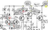
@JoseHH i think i've made some progress - I've been re-checking all the voltages on the right side of the power amp board

R34 appears to be bad (voltage is correct on one side and reduced by ~half on the other).

edit: nope. supposed to be 1.2k and it measures 1.2k. i'll keep measuring adjacent resistors until i hopefully find something bad
 

Attachments

  • Screen Shot 2023-12-06 at 3.50.09 PM.png
    Screen Shot 2023-12-06 at 3.50.09 PM.png
    322.8 KB · Views: 12
Last edited:
Ok. The resistors I suggested are all ok then. But the resistors @skippy124 sugested gave you some strange results in my opinion. To me it can not be that R05 has zero volts on both pins, and at the same time, R17, (which shares a direct conection with one of the pins of R05) gave you +27V.
On the other hand, you got zero volta for either pin of R06 and at the same time R18, which is connected to R06, you get -27V.
Something is inconsistent there don't you think?

The common point of R05 and R17 should be at the (positive 18V) voltage of the cathode of zener diode ZD603
The common point of R06 and R18 should be at the (positive 18V) voltage of the cathode of zener diode ZD605

Can you check again the voltages?. If I were to do this, I would do this on the component side to be sure that I hook the grabber onto the right pins and avoid reading at an incorrecto point.
I'll re-measure as per your advice.
 
Back
Top Bottom