• Please note that Audiokarma will be offline briefly for updates early on Monday morning, September 28th.

Scott R75s rebuild questions

Here are the caps on the Tone Control. I welcome thoughts on replacement values.
I've listed the ceramics, but don't plan to change them unless it seems important. The tone board is wired directly to a harness and I want to minimize disruption.
As always, thank you for the advice. (Hopefully I've learned to distinguish signal and power better than last round....and hmm, power caps are all marked 6xx...aha!)

Symbol/Value/(type)Signal or Power Proposed replacement type and increased voltage if any.

C1/101 .033uf (Film) S
C2/102 .0027uf S
C3/103 2.2uf 25v (tant box?) Wima PET
C4/104 22uf 25v S Muze BP
C5/105 220 6v S Muze BP 25v
C7/107 22uf 25v S Muze BP
C8/108 1uf 25v (tant box?) Wima PET
C9/109 330pf S
C10/110 180pf S
C11/111 .1uf Film S
C601 220uf 35v P Nichicon UPM 50v
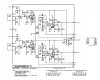
r75sToneControl.jpg
 
Last edited:
It looks like NP0 ceramics were used for values ≤47pF; this may have been the upper limit of what was available as NP0 back when this unit was manufactured. Nevertheless, the fact that they use NP0 ceramics at all is indicative of a high quality build, as is the use of glass epoxy PCBs.

It really does have amazing quality. So many labor hours must be in it. Even the chassis must have taken hours. Heavy gauge aluminum. All holes drilled, many squares and rectangles stamped out. There are many of these b/c of the daughterboard pin connectors. All deburred. Some countersunk. Final uniform belt sand on blank, then brake-bent into shape. It's a bit gratuitously nice. That final uniform planishing is just not necessary. The heatsinks likewise--drilled, deburred and ground before anodizing. In an age before CNC mills, this must really have employed a factory full of labor. The point to point wiring isn't always beautiful, but other than that it's really hard to find a cut corner.
 
Last edited:
Your analysis is correct, the additional local decoupling capacitors are to isolate the differential input signal from being modulated by the power supply sag during heavy current demands from the output stage.

Ok. My plan is to move the decoupling caps back onboard. From sharing one 1000uf filter cap, each board will have its own 1000uf. That will save the hassle of trying to wire a radial to replace the axial underneath. I'll leave the large large chassis diode in place. I'll document all that when the time comes.
 
Nichicon PM has generally lower ESR so I'll switch from PW to that for power caps.

Nichicon PW is fine, no need to switch specifically to PM; any low ESR type from a reputable brand (e.g., Nichicon, Panasonic, United Chemicon...etc...) is more than adequate compared to what was originally installed.
 
Ok. My plan is to move the decoupling caps back onboard. From sharing one 1000uf filter cap, each board will have its own 1000uf. That will save the hassle of trying to wire a radial to replace the axial underneath. I'll leave the large large chassis diode in place. I'll document all that when the time comes.
Since each board is already drilled for a diode (but not installed), consider using a soft-recovery type diode (e.g., UF4004) on each.
 
Here are the caps on the Tone Control. I welcome thoughts on replacement values.
I've listed the ceramics, but don't plan to change them unless it seems important. The tone board is wired directly to a harness and I want to minimize disruption.
As always, thank you for the advice. (Hopefully I've learned to distinguish signal and power better than last round....and hmm, power caps are all marked 6xx...aha!)

Symbol/Value/(type)Signal or Power Proposed replacement type and increased voltage if any.

C1/101 .033uf (Film) S
C2/102 .0027uf S
C3/103 2.2uf 25v (tant box?) Wima PET
C4/104 22uf 25v S Muze BP
C5/105 220 6v S Muze BP 25v
C7/107 22uf 25v S Muze BP
C8/108 1uf 25v (tant box?) Wima PET
C9/109 330pf S
C10/110 180pf S
C11/111 .1uf Film S
C601 220uf 35v P Nichicon UPM 50v

View attachment 1178028

Suggestions:
C1/101: 0.033µF (upgrade to polypropylene type, e.g., ECW, MKP, PHE426)
C2/102: 0.0027µf (upgrade to polypropylene type, e.g., ECW, MKP, PHE426)
C9/109: 330pF (replace with C0G type if not already NP0 or mica)
C10/110: 180pF (replace with C0G type if not already NP0 or mica)
C11/111: 0.1uF (upgrade to polypropylene type, e.g., ECW, MKP, PHE426)
C601: 220µF 35V increase capacity (e.g., 470µF)
 
On board C2/102 22uf 10v 22uf .6v Signal 5mm Muze BP UES1E220MEM...I just want to double check this. Replace 22uf electrolytic with a 1uf film.

Short answer: correct.

Long answer: C2/C102 forms a high pass filter with the input impedance of TR02/TR102 (BC109C). The input impedance is approx. hFE (BC109C) x emitter resistance: 420 (minimum) x 1000 ohms= 420 kohms. The target F3 for a highpass filter for a passband with a 20Hz lower limit is ≤5Hz (2 octaves below 20Hz); with a 1µF capacitor, the F3 is ~0.4Hz (this is sufficiently low, even when considering subsequent high-pass filters in subsequent stages (high filter cut-off are additive).
 
Short answer: correct.

Long answer: C2/C102 forms a high pass filter with the input impedance of TR02/TR102 (BC109C). The input impedance is approx. hFE (BC109C) x emitter resistance: 420 (minimum) x 1000 ohms= 420 kohms. The target F3 for a highpass filter for a passband with a 20Hz lower limit is ≤5Hz (2 octaves below 20Hz); with a 1µF capacitor, the F3 is ~0.4Hz (this is sufficiently low, even when considering subsequent high-pass filters in subsequent stages (high filter cut-off are additive).

Thanks. My apologies. That cap is currently 2.2uF as per schematic not 22uF as per my question. The printing is blurry and looks a lot like the 22uF on the preamp--can only tell the difference by comparing the spacing between the 2's.
 
Last edited:
Thanks. My apologies. That cap is currently 2.2uF as per schematic not 22uF as per my question. The printing is blurry and looks a lot like the 22uF on the preamp--can only tell the difference by comparing the spacing between the 2's.

Actually, the 2.2µF value seems more appropriate from a manufacturing cost/board space perspective as well as being more logical mathematically. The F3 with a 2.2µF is ~0.2Hz and this is follows the general rule of thumb that when the filter capacitor is an electrolytic type, a value at least 10x that of needed for the desired F3 should be used to minimize the distortion within the passband.
 
AFAIK, it only the (emitter) resistor to ground that is relevant; R4 is a feedback resistor.

Not sure I completely follow the logic yet (I was thinking of R4 as feedback, but also part of biasing for TR02), but it points me in the right direction - back to the books - thanks :thumbsup:
 
Actually, the 2.2µF value seems more appropriate from a manufacturing cost/board space perspective as well as being more logical mathematically. The F3 with a 2.2µF is ~0.2Hz and this is follows the general rule of thumb that when the filter capacitor is an electrolytic type, a value at least 10x that of needed for the desired F3 should be used to minimize the distortion within the passband.

Sorry to correct myself again. On the preamp those are 22uf, not 2.2uf. They are square polarized as described in this linked conversation here. Physically identical to the 2.2uf on the Drivers and in the linked pic which is the tone board. But in this circuit they are 22uf.

IMG_0517.jpg
 

Attachments

  • image.png
    image.png
    125.2 KB · Views: 3
Last edited:
I'm running through the driver boards again, trying to figure out what is going on with the bias adjustment. One barely reaches .20 mV even when turned to its extreme. It will only get there after 10 minutes of warm up.

The trimpots are in spec and work as expected when adjusted. (275 spec, Good board 520, weird board 318)

I want to include likely problem components in my parts order.

I've studied the schematics and tried to imagine what the problem could be.
My candidate problems are:
If C6 or C10 aged in a way that seriously decreased ESR that could pull the bias voltage down.
If D3 functioning as a thermistor were off, that could pull the bias voltage down. (Long warm up a clue? But i've switched the boards and the weird one is weird with any side's D3)
If TR 5 and 6 protection circuit (?) were leaking or something that could cause problems. (None of their resistors seems off.)

I adjusted both boards for .02V bias, then went through the schematic and measured all of the voltage points to ground. (All voltages listed good board first, weird board second).

The most striking discrepancy was on the negative side of D3 (Pin 6 on schematic) .561 vs. .000V I could correct this by turning the bias pot to about where the good board was located. But when I did that, the actual bias reading across R20/R21 dropped to negative.


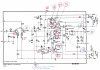
I attach a scan of the schematic. I've listed the voltage readings for each point in red. I've used blue ink to circle test points that seem particularly off. I'd welcome any suggestions about what might be going on here.
Driver voltages copy.jpg
 
Last edited:
Going back to your post # 52 - you noted previously some 'strange' behaviour for one of the dual diodes (D3), the behaviour you're seeing now with bias setting is quite possibly another manifestation of the same thing. I wonder if one them is not faulty.

AFAIK, the 'usual' replacement for 'double diodes' in this sort of position / function, is normally 2X 1N4148 mounted in series. As your D3's are remote mounted in/on the heat-sink, you could just disconnect the problematic one by desoldering the leads at the pcb end, and replacing them by 2 1N4148 in series directly on the pcb - it obviously wouldn't be thermally coupled to the heatsink like that, but it would be a 'quick & dirty' way to check if your D3 is the problem. If it is, then you'd need to look at replacing D3 properly.
.
Otherwise, considering the board is still original, the rest of your values look pretty good to me.
 
Going back to your post # 52 - you noted previously some 'strange' behaviour for one of the dual diodes (D3), the behaviour you're seeing now with bias setting is quite possibly another manifestation of the same thing. I wonder if one them is not faulty.
...
.
Otherwise, considering the board is still original, the rest of your values look pretty good to me.

Thanks, I'll keep studying the D3 connection as you suggest and see if that's the problem.
As for the values, the negative voltage on pin 13 (-.007V), which is the Collector of the PNP power transistor struck me as odd. But I'm not very knowledgable and am still getting used to thinking in +/-/ground circuits.
 
With the amp 'idling' (vol zero, no input, controls centred, etc.), you should ideally have DC-Offset voltages, of 0V DC, at the mid-point between the emitter resistors - so at the junction of R20 & R21 (effectively terminal # 10).

From your diagram, your DC Offsets seem to be +7mV and -18mV, both of which are within the spec. of +/- 25mV (see note 5 on the schematic, page 44). It just means that the ideal '0' balance point is slightly displaced - in one case towards the -ve rail, and in the other towards the +ve. Some amps have trimmers to adjust the DC offsets, yours doesn't, but values of +7mV and -18mV are both fine, so I'd leave them as is, at least until the double diodes are checked, and everything else is rebuilt. If you do subsequently need to adjust the DC Offsets, it is possible, but then you'd probably be looking at replacing the input diff. amp transistors TR1 & TR2 on that board, for a better 'matched' pair (#).

The value of -7mV at pin 13 is simply the DC offset of that amp + half of the 22mV drop you set for the bias, so -18mV + 11mV = -7mV

(#) Looking back at your earlier photos, TR1 & TR2 on one driver board look different to their equivalents on the other board - so they may have been changed previously (?). Might be interesting to check what all 4 of them are.
 
I'm running through the driver boards again, trying to figure out what is going on with the bias adjustment. One barely reaches .20 mV even when turned to its extreme. It will only get there after 10 minutes of warm up...

Is the ".20 mV" a typo, i.e., should be 20mV or 0.02V? Assuming that is the case, the 10 minute delay after power turn-on is not unusual, in fact waiting 15-30minutes for voltages/temperatures to fully stabilize is recommended.

...
I've studied the schematics and tried to imagine what the problem could be.
My candidate problems are:
If C6 or C10 aged in a way that seriously decreased ESR that could pull the bias voltage down...If TR 5 and 6 protection circuit (?) were leaking or something that could cause problems....

AFAIK, a very low ESR for C6 or C10 wouldn't affect the bias; maybe you are referring to C6 or C10 "leaking" DCV, which would increase the measured DC offset. I think the same effect would occur if the protection circuit transistors TR5/TR6 had leaky junctions.

...If D3 functioning as a thermistor were off, that could pull the bias voltage down. (Long warm up a clue? But i've switched the boards and the weird one is weird with any side's D3)

Agreed, a problem with D3 would impact the bias, but since the problem followed the driver board and not D3, it doesn't appear that D3 is faulty.

...The most striking discrepancy was on the negative side of D3 (Pin 6 on schematic) .561 vs. .000V I could correct this by turning the bias pot to about where the good board was located. But when I did that, the actual bias reading across R20/R21 dropped to negative.
What was the actual bias reading? If the +ve and -ve probe locations were switched with each other does the bias read as positive.
 
Back
Top Bottom