• The move to the new server is done. There are some software and database maintenance updates in process. This has us passing the hat around to help out. We appreciate any donations. Seriously, even a dollar helps. The payment page may be found here - https://www.audiokarma.org/support.html

SX-737 power amp AWH-033 issue, blown transistors

Next test was this morning with a little change. I got two DMM so connected the first for the bias onto pin 1 (black lead) and pin 2 (red lead) set to automatic DC-Scale.
The second one was clipped with red on pin 3, black to ground.

Then power up on DBT. The bias was at ZERO in the beginning, after a few minutes I increased VR1 careful from 0 to 20mV. With this increase the voltage at pin 3 changed to -26mV, I guess that is correct and had to be readjusted at a later stage if everything else work correct.

Second test without DBT on full power, bias was at 21mV and pin 3 at -25mV. With the bios adjustment to 20mV the voltage on pin 3 got down to -24mV

Now if I hear nothing else, I will reinstall the Q6, Q8 and Q10 for the D2 Side and test it later with my rebuild stv-4h replacement.

Excellent, bias should be Zero until you adjust it, starting with VR3 at minimum, that is why it is set that way.
The bias adjustment and the dc offset adjustment will interact, so readjust VR3 to re-establish 0vdc at pin 3, then recheck/readjust bias VR1, repeat until both are correct and stable.
What did you use to build the replacement for D2? Can you post a picture, please?
 
Bevor I started to the Q6, Q8 and the rest on that side, I checked the connection between some of the new solder points in the area around VR1. Doing so, I figured out that there was no contact between the collector of Q7 and pin 32/33 and found a bad/burned trace just between.

To fix that I soldered a wire from pin 33 to the solderpoint of c13. But with that change, and lucky for me that I did a first test with DBT, the light bulb will not dim down as it should be. So I assume that my bias adjustment befor couldn’t be right either.
At the time I’m a bit clueless.
 
Last edited:
Bevor I started to the Q6, Q8 and the rest on that side, I checked the connection between some of the new solder points in the area around VR1. Doing so, I figured out that there was no contact between the collector of Q7 and pin 32/33 and found a bad/burned trace just between.

To fix that I soldered a wire from pin 33 to the solderpoint of c13. But with that change, and lucky for me that I did a first test with DMT, the light bulb will not dim down as it should be. So I assume that my bias adjustment bevor couldn’t be right either.
At the time I’m a bit clueless.
Probably have bias (VR1) set too high now. Turn VR1 back to minimum resistance and try on DBT again, if it still will not dim there are more problems. If it does dim, while still on DBT, adjust VR1 to verify it will still control bias, then return it to minimum resistance. It is not possible to set bias correctly on DBT, but you can verify circuit function. You will also have to readjust DC offset. Post results.
 
Merlyn your step by step approach is exactly what I need.

I turned VR1 again to minimum, started with DBT and it dimmed, well so far. Next step with both DMM connected as before and I found the dc offset around 100mV, but could readjust VR3 to re-establish 0vdc at pin 3. Then bias again up to 20mV for a while. The DBT stayed dimmed during the whole procedure.

Then everything again on full power with some minor the adjustment on VR1 and VR3 for the required values.

One other basic question popped up. Would you recommend before every soldering work on the board to discharge the two big caps? Every time I touch the collector soldering point on Q7 and Q8 I get a little spark, because pin 32 and 22 are connected to the big caps.

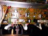
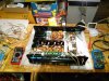
That’s how my setup looked like.
IMG_20190811_174814.jpg
Now I can continue with the D1 (STV-4H) workaround.
 
Last edited:
Remember to turn bias back down when set on DBT BEFORE powering up on full AC mains. Once it is set correctly on Mains you can leave it set there.
Would you recommend before every soldering work on the board to discharge the two big caps?
Yes, that should be standard procedure, otherwise component damage may occur if it discharges through a part than cannot handle the current.
Some units have a load resistor across them (the big caps) from the factory, and sometimes people will add them as an upgrade.

It was the D1 (STV-4) workaround I was hoping for a picture of, major steps as you build it and when it is finished.
 
Is it correct that one can only adjust the bios with the output installed?

Yes I know you wait for pictures on the D1 (STV-4H) workaround. My first attempt didn’t work or I made a mistake during the test with the 9V battery because it got so hot, the solder joints came apart. Now I’m working on a second version. Right now, there are three n4148 soldered in line and connected to the board, hanging free in the air, just that I can test the dc offset is working.
IMG_20190811_201450.jpg

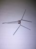
As you can see on the picture, I had a piece of metal with slightly folded sides and three n4148 soldered together. The diodes will been fixed with epoxy inside.

IMG_20190810_142940.jpg IMG_20190810_160849.jpg I will send more pictures as soon as I have a working part.
 
Last edited:
Is correct that one can only adjust the bios with the output installed?
That is correct, the bias overcomes the crossover distortion that occurs in a pure Class B output configuration and puts the transistors into a more linear conduction region. It flows through the collector of the positive supply side transistor, the emitter, the positive side emitter resistor, the negative side emitter resistor, the neg side emitter, the neg side collector and the negative supply. It is set by the voltage across the STV and the VR. The STV compensates for temperature variations in the output transistors. A pn (base-emitter or diode) junction's voltage decreases as it gets warmer, so for a constant voltage across it more current flows. In a transistor more base current causes more collector current, which causes more power dissipation, which causes more temperature rise. If this is not controlled the transistor goes into 'thermal runaway' and fries itself. The STV mounted on the heatsink decreases its junction's voltage drops as its temp rises, thereby decreasing the DC voltage across the output transistors B-E junctions and stabilizing the bias (idle) current. The heatsink provides the thermal connection between the STV and the output transistors. Don't try to set bias without having the STV, or its substitute, attached to the heatsink. The DBT limits the input power and protects the output transistors (briefly) from thermal runaway caused by excessive bias current as one of its functions, you saw the bulb stay bright with the bias set too high. That would have damaged the output transistors and maybe other parts without the DBT.
That looks like a good start on the STV sub. Some heat-shrink on the leads and encase it in epoxy and it will be ready to test. Monitor the temperature and the bias closely to be sure it tracks correctly.

EDIT: more info
 
Last edited:
I promised to post pictures with the STV-4H workaround and here we go.

The basic for all my four attempts are three n4148 in line. With 3 times 0.7V you get 2.1V in total which is very close to the 4 x 0,55V in the STV-4H.
But the three single n4148 need more space so everything you build will be at least three times bigger than the original.

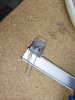
My first and second try was with a thin piece of metal, slightly folded up on the side, only to keep the epoxy in place as good as possible. It was necessary to avoid every contact between the connecting leads and the metal case, so the short leads between the diodes were bend a bit upwards and cut leaving a length between 2-3mm left. The two leads on both ends will stay.

With this preparation done, I mixed a small amount of my two component epoxy-clue, put it on the metal where I later want to position the diode. Not too much, otherwise the glue will run to each open side. Then you wait a few minutes until the clue gets more sticky and now you can carful place the diodes on the metal blade and correct the position as you like. You have to make sure, that none of the leads will touch the surrounding metal, the glass housing of the diode is OK. I did tilt the long legs a bit and kept them away. If you find it better for you, put it on tooth pigs or chopsticks to keep it a bit lifted away.

After some time, if you find the epoxy solid enough, you will put a second layer on top, just do cover the open leads. It may take a few hours (8-12) until the epoxy hast hardened enough, so you can work on it.
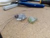
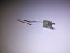
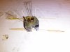
My first attempt look not very good, rather messy but it did basically work. It is that “funny something” left on the front. The brown part on the right is the original STV-4H.
IMG_20190811_210337.jpg IMG_20190812_181415.jpg
My next plan was to build a case with a flat and solid side, so I get a very good contact to the heat sink. I bought an alum U-profile with 1.5mm thickness and 10mm space between the legs.

Tools used. Dremel with small cutting disc, drill 3.5 mm, small file, flat pliers

First I drilled the 3.5mm gap for the screw, then cut with the dremel both wings on the side with the hole very close to the bottom as you can see on the picture. The length of the cut must ensure, that you have still enough space for the screw head. It’s up to you which side you bend inside and/or where to you cut off the excessive rest. That is only necessary to keep the epoxy in position.

As an extra isolation, I used a small plastic strip, cut and bend with the help of a hot knife, just to fit to the side off the metal. On one of the picture I have the side wings at full height, but it didn’t look to good. Since the diode didn’t need more than 4-5mm in height, I decided to reduce the sidewalls to get a more handsome look at the end.

After finishing the metal case, you can start with the epoxy as described before.
IMG_20190812_181910.jpg IMG_20190812_182013.jpg IMG_20190812_182528.jpg IMG_20190812_182850.jpg IMG_20190812_182858.jpg
Now the glue should have time to harden and tomorrow I will test it with the SX-737

 
Last edited:
So far my latest self-made STV-workaround looks quite good, only some minor improvements necessary.
Late afternoon, after work I will have the first test. One side (left) with the original STV-4H and right side with the replacement, attached to the heat sink.

A few questions before. Shall I mount it with thermal component? To you agree with my planed test steps or what would you recommend?

I will start with these steps, always two DMM connected to indicate the dc offset and bias values.
  • First everything on DBT and outputs NOT installed. VR1 set to minimum, then check and adjust dc offset to 0.0mV on VR3.
  • Next try with outputs plugged in and fixed. Again VR3 recheck and then slowly VR1 set to 20mV.
  • If that works fine, I will go to full power and let it warmup for some minutes, readjust VR1 and 3 and watching the dc offset and bias values.
  • Last test will be a crosscheck on both sides for dc offset, bias values and monitoring the temperature while playing some music.
Anything else I have to take care?
Finally I will report how it went.
 
So far my latest self-made STV-workaround looks quite good, only some minor improvements necessary.
Late afternoon, after work I will have the first test. One side (left) with the original STV-4H and right side with the replacement, attached to the heat sink.

A few questions before. Shall I mount it with thermal component? To you agree with my planed test steps or what would you recommend?

I will start with these steps, always two DMM connected to indicate the dc offset and bias values.
  • First everything on DBT and outputs NOT installed. VR1 set to minimum, then check and adjust dc offset to 0.0mV on VR3.
  • Next try with outputs plugged in and fixed. Again VR3 recheck and then slowly VR1 set to 20mV.
  • If that works fine, I will go to full power and let it warmup for some minutes, readjust VR1 and 3 and watching the dc offset and bias values.
  • Last test will be a crosscheck on both sides for dc offset, bias values and monitoring the temperature while playing some music.
Anything else I have to take care?
Finally I will report how it went.

I like the idea of thermal compound for mounting the STV and sub. I am going to do that when I rebuild my SX-1050, it has STV-3 varistors.
Remember to reset bias VR1 to minimum after verifying circuit function on DBT, before going to full power. :rolleyes:

You will have to stop the music input to check dc offset and bias, of course. :)
Looks like you have it figured out! :thumbsup:
 
Hello again, I could finish work earlier and continued right away with preparing my self-made STV-sub. For the next example I will have to make sure the position of anode and cathode in relation to the mounting position. For the original it doesn’t matter because you can just turn it every way you need before you fix it on the heat sink.
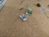
IMG_20190813_171649.jpg
With my sub you better take care how the leads will run, before you place it in the case, because the best mounting position is with the leads going on top.On the SX-737 left and right side are different, so it would better fit for the left side.

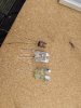
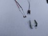
As you see on my picture, the leads will cross and could produce a short if they get in contact. But for the test I arranged the leads and will change the leads layout afterwards.

IMG_20190813_172513.jpg IMG_20190813_172551.jpg

To have a better idea if and how the sub worked, there are some values I measured before.
The original STV-4H hat 2,1vdc and 36pF, my sub hat 2.06vdc and 0pF on the small LCR-T4 tester.

After the sub was in place I started the test sequence as mentioned above and everything worked fine. I had the two DMM hooked up for dc offset with red on pin17 and black to ground. The second one with red on pin 18, black on 19.

Then test with DBT, followed with outputs in and finally on full power.
No big changes had to be made, adjustment went much better than expected.

Dc offset on both sides around 0.05mV and bias set around 20mV even after a short worming up. Unfortunately I can’t find my IR laser to check the temperature, the heat sink was still very cold.

You will have to stop the music input to check dc offset and bias, of course.
Merlin I didn’t read your advice in time before switching the tuner on an listening to the music with the headset. Lucky for me, nothing went bad.

During the whole time I had both DMM connected and running. The dc offset on the sub side went up a bit to 2mV but I assume that's still in limit! Or what’s your opinion?

After 30minutes on tuner I had to stop for dinner but would like to make a much longer system check with tuner on.

Any advice for that?
If everything works fine, I will continue with the tuner board and the last three left.


Now lessons learned for everyone who want’s to rebuild the sub. Make a drawing how you want to mount it on the heat sink, mark the position of anode on the board and check how the diode has to sit inside the case to avoid crossing leads afterwards.
 
Last edited:
My internet connection was down all day yesterday until past midnight :(.
That is very nicely done. Wonderful photos and documentation! As a suggestion a bit of heat shrink tubing on the leads up against the body, then a bit more epoxy to attach the heat shrink to the body would better protect them from shorting and breaking.
As for testing the real effectiveness of the substitution, that will not happen until you run it loaded (speakers or dummy) with the volume up enough to warm the heatsink.
 
Very good idea with the heat shrink. I will build another one with long enough legs, colored heat shrinks to mark red and black and fix it inside the epoxy as you advised. :beerchug:

Merlyn you wrote in no. 16
“When we get to functional testing we will compare D1 and D2 in circuit with the power on (not on test jig).”
Is there anything I can to in the meantime?

My unprofessional plan for a real test is like that: For now I have my hand on four DMM :)
Preparing both sides with alligator clamps on cable on all pins for dc offset and bias.
Connecting the four DMM on the pins for dc offset and bias and have them switch on for the whole time. Then power up and let it run on tuner with a usual volume on speakers. In a sequence of 10 minutes I check the temperature with an IR laser and take the values from my DMM. That procedure will take place for at least one hour, so I have a few values to compare later on a list.

Does that sound OK or what else would your suggest for a comparison test between D1 and D2.
 
Last edited:
Very good idea with the heat shrink. I will build another one with long enough legs, colored heat shrinks to mark red and black and fix it inside the epoxy as you advised. :beerchug:

Merlyn you wrote in no. 16

Is there anything I can to in the meantime?

My unprofessional plan for a real test is like that: For now I have my hand on four DMM :)
Preparing both sides with alligator clamps on cable on all pins for dc offset and bias.
Connecting the four DMM on the pins for dc offset and bias and have them switch on for the whole time. Then power up and let it run on tuner with a usual volume on speakers. In a sequence of 10 minutes I check the temperature with an IR laser and take the values from my DMM. That procedure will take place for at least one hour, so I have a few values to compare later on a list.

Does that sound OK or what else would your suggest for a comparison test between D1 and D2.

I think that is a good idea, here is my step-by-step procedure:
To compare D1 and D2 I would monitor the voltage across the Diode and the Bias at the same time on both channels. You can only do this when the amp is not playing music because the changing sound makes the measurements change along with them. Have the meters hooked up, shut off the input, quickly record the measurements.
Measure and record voltage and bias for both channels:
Immediately after power on with the unit at room temp (cold).
After 10 to 20 minutes sitting idle and stabilized (no sound playing).
After about 10 minutes playing at low level with a normal load (speakers or dummy) or until heatsink temperature stabilizes.
After about 10 minutes playing at moderate level with a normal load (speakers or dummy) or until heatsink temperature stabilizes.
After about 10 minutes playing at high level with a normal load (speakers or dummy) until heatsink temperature stabilizes. This is the step where the risk of thermal runaway occurs if the substitute does not manage bias safely. High level means to me at the greatest volume I would listen to, not the maximum amps output. If the bias increases too much turn it down a bit.
If it all looks good, maybe input a 400Hz or 1kHz sine wave, use dummy loads, increase output to just below clipping, and do a max power test. This is a really risky test, and not necessary for listening pleasure, but will prove all your repairs/changes to the power amp section are working. This kind of test, with a sine wave, is very stressful on the amp, don't leave it unattended. Most amps will not tolerate this for long (even a few minutes) without overheating.
As an option record room temperature and heatsink temperature for every reading.
This process is fairly labor intensive. I built a pair of custom replacements (thanks to rcs16 & hbrown) for the STK-0050 power output IC in an SX-780 and did a similar test to proof them. Search for SX-780 and STK-0050 on AK for more info on these if you are interested, there is a long, very detailed, educational thread with many AKers involved.
 
Last edited:
If I can manage it, I will set up the test today.
There only one thing I’m not sure where you exactly take the voltage.
You wrote
“To compare D1 and D2 I would monitor the voltage across the Diode….”
Does it mean on the left and right side of the D1/D2 or did you mean the normal pins for the dc offset.

If you mean direct on the D1/D2 than I will solder an extra lead to the STV legs on the foil side going to the DMM, just to prevent a short circuit what easily could happen so close to the heat sink.
 
If I can manage it, I will set up the test today.
There only one thing I’m not sure where you exactly take the voltage.
You wrote

Does it mean on the left and right side of the D1/D2 or did you mean the normal pins for the dc offset.

If you mean direct on the D1/D2 than I will solder an extra lead to the STV legs on the foil side going to the DMM, just to prevent a short circuit what easily could happen so close to the heat sink.

Across the diode, to monitor and compare the voltage drop across the diodes, to see how it changes according to temperature. Any physical point that is electrically the same will do. In this case it does not have to be physically at the diode unless that is the most convenient. DC offset will not change significantly unless there is a failure, or over a long period as components age. It is controlled by the differential amp at the beginning of the power amp stage, which is not subjected to the temperature changes like the output transistors on the heatsink. Recheck it periodically, it would be an interesting data point if you feel the need to monitor and record it. I do not think it worth interrupting the test to measure DC offset and moving DMM leads. Since you have 4 DMMs connect them and leave them connected as you progress through the steps, you do not need to risk shorting something moving the leads while the power is on, and shutting power down between steps to move leads safely breaks the progression and let the unit cool off between steps.
The link in post #25 is related to this process, we are reconfirming that his experience 'in the laboratory' works for you on your unit in real world conditions.

EDIT: update, more info
 
Last edited:
Today I set up everything for the test of the power amp with the STV sub, but it wasn’t very successful.

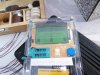
Left side was the original STV (D1) and on the right side my STV-sub (D2) made out of 3 x N4148. To take the voltage, I use extra leads soldered to the legs of D1 and D2, each connected to a separate DMM the full time.
IMG_20190816_204855.jpg
Then leads to the pins for dc offset and bias.

The room temperature was 20 ° Celsius.
The first reading after start with aux selected, I had 2,2V across D1 and only 1,18v at D2. DC Offset was good on both sides.

After 15 minutes I switch to tuner and turned the volume up to a low level. From the start I had a very quiet right channel. To rule out the speaker I made a check with a headset as well as a change with the speaker, the right channel was still very quiet. So I tried on the balance but no chance, later as I turned the volume up the right channel came on and stay at the same level as the left side for a while, even when I turn down the volume again. But only for a short time, than the right side went down again.

During the whole time, the voltage of D1 and D2 stay very close at the values measured at the start, as well as the dc offset.
IMG_20190816_213408.jpg
After about 40 minute the right channel stayed very quiet, even at a higher volume selected. So I stopped the test at that point.

What leaves me confused, all dc voltages stayed close to the start values on both sides.
The temperature on the heat sink slowly increased from 20 to 29°C measured at D1 and D2.

Initially I though the problem with the right channel might come from the switch and volume circuit, but now I’m not sure at all.
So far the control amplifier and the switch and volume circuit are untouched.

What I don’t understand either is the low voltage with the STV-sub. I personal expected around 2v but not 1.18v!
 

Attachments

  • IMG_20190816_204855.jpg
    IMG_20190816_204855.jpg
    101.8 KB · Views: 9
Last edited:
Back
Top Bottom