

You are using an out of date browser. It may not display this or other websites correctly.
You should upgrade or use an alternative browser.
You should upgrade or use an alternative browser.
The OFFICIAL MSM5540RS/M5540 Sansui Gx700 40pin IC Thread! NUDIES
- Thread starter trueno92
- Start date

I have nothing but admiration for your efforts so far, you seem to be very close to a solution. I think I speak for others when I say we will happily wait for how ever long it takes for your 'background processing' to bear fruit. 

(I wonder if this has been discussed on DiyAudio? )
)
Update
I have posted a thread asking for any help or insights on that Forum.
(I wonder if this has been discussed on DiyAudio?
)Update
I have posted a thread asking for any help or insights on that Forum.
Last edited:

@PE9ZZ I am not sure how far you got on this, but earlier this year I decided to poke into this as I had a T-80 tuner with a non-functional MSM5540 and enough electronics knowledge to hopefully figure out something. As with everyone else, I was not able to find a lot of information about this IC but I did stumble into the TU-719 service manual, which actually goes into great detail about how the MSM5540 works including the time cycles and counting architecture of the original chip. It also describes the tuner operation when powering on and switching from AM to FM.
I found this one particularly excellent diagram that seemed to give some meaningful information.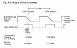
so I know that the frequency input on PIN 39 is the Local Oscillating frequency which is received frrequency + IF for upper heterodyne. And I was able to confirm this on my unit with a scope and frequency counter. So since the displayed frequency is just the pin 39 LO with the IF subtraced, plus some funky math with 0.5 to "round the results to the nearest MHz", that part is easy to get a display.
Even issuing the LOCK OUT 1 signal (pin 35) is fairly straightforward once the correct receiving frequency is obtained with some reading of pin 2-5 and some math. There is a chart in the TU-719 describing offsets that can be followed.
So again I was back to the exact problem you had, the signal the manual calls VREF_CTL (I think you called this "KILL") and the analog voltage output.
There is one line in the text of the manual that basically says if the frequency is tuned at the center frequency the TR18 will be off which will allow the value at pin 33 (VREF_CTL) to be high, then a proportional analog voltage should be emitted on PIN 32. This drives a VCO to counteract drift from the center frequency (positive or negative).
I was concerned about your suspicion that there is more timing and predictive behavior here, but we are talking about late 70's ICs here so I was hopeful it would not be that complicated.
so a few months ago I decided to implement a circuit that basically just did what was described in the diagram above, using PWM and a RC circuit to make an analog voltage.
And I was shocked to see that it seemed to mostly work. its a bit touchier than the official chip but it will display frequency, quartz lock, and seems to resist tuner drift.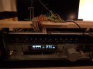
I found this one particularly excellent diagram that seemed to give some meaningful information.
so I know that the frequency input on PIN 39 is the Local Oscillating frequency which is received frrequency + IF for upper heterodyne. And I was able to confirm this on my unit with a scope and frequency counter. So since the displayed frequency is just the pin 39 LO with the IF subtraced, plus some funky math with 0.5 to "round the results to the nearest MHz", that part is easy to get a display.
Even issuing the LOCK OUT 1 signal (pin 35) is fairly straightforward once the correct receiving frequency is obtained with some reading of pin 2-5 and some math. There is a chart in the TU-719 describing offsets that can be followed.
So again I was back to the exact problem you had, the signal the manual calls VREF_CTL (I think you called this "KILL") and the analog voltage output.
There is one line in the text of the manual that basically says if the frequency is tuned at the center frequency the TR18 will be off which will allow the value at pin 33 (VREF_CTL) to be high, then a proportional analog voltage should be emitted on PIN 32. This drives a VCO to counteract drift from the center frequency (positive or negative).
I was concerned about your suspicion that there is more timing and predictive behavior here, but we are talking about late 70's ICs here so I was hopeful it would not be that complicated.
so a few months ago I decided to implement a circuit that basically just did what was described in the diagram above, using PWM and a RC circuit to make an analog voltage.
And I was shocked to see that it seemed to mostly work. its a bit touchier than the official chip but it will display frequency, quartz lock, and seems to resist tuner drift.

@princever, that's a very good find, and you seem to have found a (mostly) functional workaround. Any chance you'd publish the circuit you cooked up? At this stage, I don't worry too much about tuner anymore, but from an aesthetic standpoint, it'd be nice to have a way to maintain the frequency display on units with a failed chip, if nothing else. I expect this to be a growing problem as these units age further, and we likely see a greater number of failures in this IC's.
I'm getting there. This is a lot of typing.
So this first revision of circuit borrowed heavily from some of the work PE9ZZ had done, and had many problems, including drawing over 100ma which was badly loading down the 5V supply of the tuner, so badly that I had to drive it separately. It also was running from a raspberry pi pico, which was both overkill and problematic, being a 3.3V microcontroller. I did not have a solid schematic yet, and the level shifting was extremely problematic.
so I switched microcontroller to a ATMEGA162, with the reasoning being that it can run an Arduino compatible bootloader and I would not need any separate shift register IC's because it has enough I/O. I also decided I was not going to be programming in any Assembly Language. I did enough of that in college. I then designed everything to fit on a PCB and finalized pinout on the ATMEGA because I am using 3 out of the 4 timers on this model for delays, counting and PWM functions.
Like all the cool kids, I came up with a name for the project, the 5540+ Project. Here is a rev 1 PCB: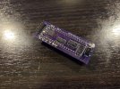
Sadly this PCB had so many problems but gave me hope that a drop-in replacement was still possible. it had clock stability issues and issues with power stability and issues driving the transistor arrays. I ended up removing the reliance on the onboard 6.5536MHz crystal oscillator on the digital display board and driving it separately from a 16MHz crystal due to frequency drift that I could not account for in the circuit. I also had a bunch of snaking traces all over the board that were picking up noise.
The rev1 board still drew too much power and I never successfully ran the tuner with this board installed.
so I started designing rev 2.
So this first revision of circuit borrowed heavily from some of the work PE9ZZ had done, and had many problems, including drawing over 100ma which was badly loading down the 5V supply of the tuner, so badly that I had to drive it separately. It also was running from a raspberry pi pico, which was both overkill and problematic, being a 3.3V microcontroller. I did not have a solid schematic yet, and the level shifting was extremely problematic.
so I switched microcontroller to a ATMEGA162, with the reasoning being that it can run an Arduino compatible bootloader and I would not need any separate shift register IC's because it has enough I/O. I also decided I was not going to be programming in any Assembly Language. I did enough of that in college. I then designed everything to fit on a PCB and finalized pinout on the ATMEGA because I am using 3 out of the 4 timers on this model for delays, counting and PWM functions.
Like all the cool kids, I came up with a name for the project, the 5540+ Project. Here is a rev 1 PCB:
Sadly this PCB had so many problems but gave me hope that a drop-in replacement was still possible. it had clock stability issues and issues with power stability and issues driving the transistor arrays. I ended up removing the reliance on the onboard 6.5536MHz crystal oscillator on the digital display board and driving it separately from a 16MHz crystal due to frequency drift that I could not account for in the circuit. I also had a bunch of snaking traces all over the board that were picking up noise.
The rev1 board still drew too much power and I never successfully ran the tuner with this board installed.
so I started designing rev 2.
Thank you for the summary (so far). An excellent effort, even if there is not much chance of a "payoff" in commerical terms. I'm not sure how many of these could be sold (assuming a final, reliable iteration comes to pass) or at what price point it would be viable, as there seems little interest these days in the matter of failing MSM5540 IC's based on the dearth of recent posts here on the subject. Seems like there was a spike in interest a few years ago that has since fallen off.
@Sansuiman I agree. I will detail a summary of the IC and other parts at the end. I suspect this would be worth something to someone with, say a G-7700+ that is otherwise perfect or restored but the chip is knackered.
So with rev2 I made some significant layout changes to the board. I hated having all the headers sticking out. the ICSP header was only going to be used once, to install the bootloader, so it seemed a huge waste. I was really hoping that rev2 would be the final design.


the benefits of the rev2 board are numerous:
- shrunk by quite a bit from the rev1 to better fit the existing DIP-40 socket
- clean and organized trace routing to reduce electrical noise
- made some changes with the way the segments were attached to the different I/O pins for super easy digit outputs
- pads on the bottom are for the ICSP for bootloader installation. all other programming is done with the UART (white connector on top)
- still a drop-in replacement with no changes needed on a F-3000 board.
These are soldered by hand and hot plate.
Here is it installed on my tuner: (I have a socket on the board. I do not think this is small enough to be directly soldered.

So with rev2 I made some significant layout changes to the board. I hated having all the headers sticking out. the ICSP header was only going to be used once, to install the bootloader, so it seemed a huge waste. I was really hoping that rev2 would be the final design.
the benefits of the rev2 board are numerous:
- shrunk by quite a bit from the rev1 to better fit the existing DIP-40 socket
- clean and organized trace routing to reduce electrical noise
- made some changes with the way the segments were attached to the different I/O pins for super easy digit outputs
- pads on the bottom are for the ICSP for bootloader installation. all other programming is done with the UART (white connector on top)
- still a drop-in replacement with no changes needed on a F-3000 board.
These are soldered by hand and hot plate.
Here is it installed on my tuner: (I have a socket on the board. I do not think this is small enough to be directly soldered.
Very well done. I hope you may consider offering these in some form eventually, but as I already said, it may be difficult to get to a "break even" with such an offering, given the limited interest, and time and effort involved in assembly. I have 6 tuners here that use the MSM5540 (TU-919 x3, TU-719 x2, T-80 x1) and somehow none have yet exhibited the failure.
I did secure a couple of spare chips back when they could still be sourced from CEI, and haven't had a need for one...yet. I really need to lighten the number if tuners I have here, but am resistant to breaking up matched sets of components. Of course, even just sitting in storage, I assume the NOS IC's could fail, since I suspect the failures may be due to the encapsulation failing and allowing either the lead wires or portions of the die to be compromised by oxidation or other external contamination.
I did secure a couple of spare chips back when they could still be sourced from CEI, and haven't had a need for one...yet. I really need to lighten the number if tuners I have here, but am resistant to breaking up matched sets of components. Of course, even just sitting in storage, I assume the NOS IC's could fail, since I suspect the failures may be due to the encapsulation failing and allowing either the lead wires or portions of the die to be compromised by oxidation or other external contamination.

A lot of activity all of a sudden! The issue that hindered my development most is the slow VCO filter time and how to switch it to fast. I just could not figure out how that worked and then I threw it in the corner. For now I'll just sit back and enjoy the show. If there are any issues you can't resolve maybe I can help out. I'm not sure I've read the explanation in the TU-719 manual but I'll look into it.
Edit: I found the confusing part to be the circuit around pin#33. This is a sort of feedback from both the micro and the analog circuitry that I just couldn't fathom.
Edit: I found the confusing part to be the circuit around pin#33. This is a sort of feedback from both the micro and the analog circuitry that I just couldn't fathom.
Last edited:
In the middle of all this I was able to acquire a F-3220 board (the one with the combined prescaler and display). I was told that the chip was dead, but somehow the MSM5440 chip on it was working fine (I put it in the socket in the T-80). We do have another receiver in the house a G-6700 which I was forbidden from taking out of the living room so I have not been able to do testing on that. The F-3220 is not a drop in replacement because all the connectors are different.
I will post more screenshots and oscilloscope views from the original chip, but suffice to say that most of what I saw matched the scope captures from PE9ZZ. But I was able to do more testing. More on that later.
So we have some huge benefits now with rev2. First, power consumption is down within a very reasonable range that the tuner +5V supply can drive it, coming in somewhere between 30-40mA depending on the exact scenario and how many segments are on. The orignal chip comes in somewhere between 18 and 25ma so we are still a bit higher but we are running a real microcontroller and not some gates and counter circuits like the original. I was able to save some power by disabling parts of the microcontroller that we are not using like the SPI and I2C hardware, etc.
Next is that it drives the display like I expect so I can start to focus on tweaking the output. I still had some clock related issues (see the bodged crystal and capacitors on the one in the tuner).
So what is working:
- FM & AM display
- correctly detecting the IF frequency selection via the diodes and jumpers and doing the necessary math
- Quartz lock (both the LOCKOUT_1 and LOCKOUT_2 signals are implemented) even though LOCK2 is not used in my tuner.
- DA OUTPUT
- the 100ms cycle that it runs on (same as original IC) this is actually about 102ms due to some extra math after a frequency count is made but I do not notice it refreshing any slower because the difference is so small.
What needs to be done?
- Testing, Testing, Testing. I have no idea if it would work on any other board other than a F-3000 in a T-80.
- rev3 board. the design is final and send to get a prototype at osh park.
- tweak the profile with which it outputs the PWM corresponding to analog voltage. its a bit aggressive but thats easily done in code and I do not believe any further hardware changes are needed.
I will post more screenshots and oscilloscope views from the original chip, but suffice to say that most of what I saw matched the scope captures from PE9ZZ. But I was able to do more testing. More on that later.
So we have some huge benefits now with rev2. First, power consumption is down within a very reasonable range that the tuner +5V supply can drive it, coming in somewhere between 30-40mA depending on the exact scenario and how many segments are on. The orignal chip comes in somewhere between 18 and 25ma so we are still a bit higher but we are running a real microcontroller and not some gates and counter circuits like the original. I was able to save some power by disabling parts of the microcontroller that we are not using like the SPI and I2C hardware, etc.
Next is that it drives the display like I expect so I can start to focus on tweaking the output. I still had some clock related issues (see the bodged crystal and capacitors on the one in the tuner).
So what is working:
- FM & AM display
- correctly detecting the IF frequency selection via the diodes and jumpers and doing the necessary math
- Quartz lock (both the LOCKOUT_1 and LOCKOUT_2 signals are implemented) even though LOCK2 is not used in my tuner.
- DA OUTPUT
- the 100ms cycle that it runs on (same as original IC) this is actually about 102ms due to some extra math after a frequency count is made but I do not notice it refreshing any slower because the difference is so small.
What needs to be done?
- Testing, Testing, Testing. I have no idea if it would work on any other board other than a F-3000 in a T-80.
- rev3 board. the design is final and send to get a prototype at osh park.
- tweak the profile with which it outputs the PWM corresponding to analog voltage. its a bit aggressive but thats easily done in code and I do not believe any further hardware changes are needed.
Consider me impressed. This goes well beyond my own knowledge, but I know enough to grasp what is being described. Would you say the additional operational data covered in the TU-719 service manual was the key to "cracking" this one? It's odd how Sansui did that sometimes, where a new concept or part like an IC would only be covered in one service manual. One needed to know this through experience as a tech, as it is never mentioned in subsequent manuals to refer back to a particular manual for more detailed information.
The XR-Q9 turntable comes to mind as a similar case; some of the information needed to service it is contained in the FSM of an earlier model (FR-Q5 I think). Of course, one would also need to have all the manuals issued to be able to do this readily. That wouldn't have been an issue for a factory authorized shop, but now 50 years on, it's not quite as easy for the DIY tech.
The XR-Q9 turntable comes to mind as a similar case; some of the information needed to service it is contained in the FSM of an earlier model (FR-Q5 I think). Of course, one would also need to have all the manuals issued to be able to do this readily. That wouldn't have been an issue for a factory authorized shop, but now 50 years on, it's not quite as easy for the DIY tech.
I agree with that statement. I would not have been able to decipher the Pin 32 and 33 behavior without the descriptions in the TU-719 manual.
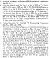
The key was this section:
So basically this happens:
When we are at a center frequency (every 100kHz +/- 20kHz) the chip outputs a lock signal on PIN 35. When we are receiving a strong enough signal it will light the lock LED and then TR16 turns on and TR18 turns off which means the internal pullup resistor of the MSM5540 will pull pin 33 high, so it emits an analog voltage centered at 2.5V proportional to how far away we are from the center frequency. When we are not tuned, TR16 will be off and TR18 turns on, grounding pin 33 of the chip. When we see a low level at PIN 33 just output 2.5V analog voltage from PIN 32 DA OUT.
as far as the Fast or Slow behavior, it really seems to be dependent on how fast the frequency changes based on the variable capacitance diode they are using. But just monitor it every 100ms and adjust the PWM to get the needed analog voltage out and as the frequency changes, it will change quickly if it is at the edge of the range, but after half a second or so it will be closer to the center of the range so it will make less drastic changes.
One thing to note is that I think they are using some sort of switched resistor divider in the original IC. There appears to be about 10 unique analog voltage levels it produces between 0.5V and 5V. The voltage coming out is too clean and perfect for any PWM type circuit to be running.
My circuit produces a noisier signal with the PWM, but it does go through several stages of low pass filter RC circuit on board, one before the op-amp with a 1uF capacitor and resistor, and one in the tuner so I think that is why it still works okay.
The key was this section:
So basically this happens:
When we are at a center frequency (every 100kHz +/- 20kHz) the chip outputs a lock signal on PIN 35. When we are receiving a strong enough signal it will light the lock LED and then TR16 turns on and TR18 turns off which means the internal pullup resistor of the MSM5540 will pull pin 33 high, so it emits an analog voltage centered at 2.5V proportional to how far away we are from the center frequency. When we are not tuned, TR16 will be off and TR18 turns on, grounding pin 33 of the chip. When we see a low level at PIN 33 just output 2.5V analog voltage from PIN 32 DA OUT.
as far as the Fast or Slow behavior, it really seems to be dependent on how fast the frequency changes based on the variable capacitance diode they are using. But just monitor it every 100ms and adjust the PWM to get the needed analog voltage out and as the frequency changes, it will change quickly if it is at the edge of the range, but after half a second or so it will be closer to the center of the range so it will make less drastic changes.
One thing to note is that I think they are using some sort of switched resistor divider in the original IC. There appears to be about 10 unique analog voltage levels it produces between 0.5V and 5V. The voltage coming out is too clean and perfect for any PWM type circuit to be running.
My circuit produces a noisier signal with the PWM, but it does go through several stages of low pass filter RC circuit on board, one before the op-amp with a 1uF capacitor and resistor, and one in the tuner so I think that is why it still works okay.
Excellent, that appears to operate so close to original as to be indistinguishable to me (comparing directly to a T-80 with a real MSM5540 installed). Is the operation of the signal strength and center tuning indicators handled by the 5540 as well, or are those inputs sent separately to the VFD? I've never looked that closely at this setup, though the TU-719 is probably very similar overall, as it uses the same VF display (along with the G-x700 receivers). The TU-919 uses a red LED 7 segment display (with kHz and MHz indicated by micro bulbs behind a red lens meant to match the LED's). Signal and center tuning meters are both analog meter movements, and not part of the digital display.
Also consider me impressed, the above describes me too. This is a magnificent piece of work.Consider me impressed. This goes well beyond my own knowledge, but I know enough to grasp what is being described.
Not forgetting the excellent work by @PE9ZZ, without whose groundwork this may never have been investigated further.
Last edited:
This is done by IC04 (BA658).Is the operation of the signal strength and center tuning indicators handled by the 5540 as well, or are those inputs sent separately to the VFD?
Don't know what else to say really. Incredibly innovative reverse engineering on both your parts...