

You are using an out of date browser. It may not display this or other websites correctly.
You should upgrade or use an alternative browser.
You should upgrade or use an alternative browser.
Yamaha M-80 Protection/Restoration
- Thread starter RyeGuy859
- Start date


Asmodeus2112
Super Member
Curious what BCE is of TR168


RyeGuy859
Well-Known Member
Yes I have bothDo you have a KSC1815 or a KSC2383.. Replace TR168..
E 0v C 37v B .005VCurious what BCE is of TR168
Asmodeus2112
Super Member
What are the voltages on both sides on R208 and R213?
RyeGuy859
Well-Known Member
I tightened all 3 screws that attach to copper pads.
Remind you this is on a dbt with a 200w bulb.
37.94v 36.3v(TR168 side) R208 Voltage drop of .006v
36.33v(TR168 side) 36.36v R213 Voltage drop of .016v
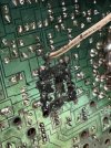
Thought i was onto something as i found more solder joints under there foam but after removing the foam and resoldering them nothing changed.
Remind you this is on a dbt with a 200w bulb.
37.94v 36.3v(TR168 side) R208 Voltage drop of .006v
36.33v(TR168 side) 36.36v R213 Voltage drop of .016v
Thought i was onto something as i found more solder joints under there foam but after removing the foam and resoldering them nothing changed.
Attachments



Sparkplug
Super Member
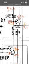
Fine, what voltages do you get at the red dots below,Just finished touching up every joint on the main amp board and the two power boards on top. Still no change.


Sparkplug
Super Member
Tr143c is way off, also b-e voltage is low, the transistor is off. Is the solder work okay? Is C171 healthy?
Emitter and base voltages are somewhat high, may or may not be an issue (probably not). I’d take voltage measurements of all that section, bias current detector, etc. included, to have a voltage map of what’s going on.
If Tr143c is disconnected from the D146(?) it’s feeding, what happens, does Tr143c voltage change?
Emitter and base voltages are somewhat high, may or may not be an issue (probably not). I’d take voltage measurements of all that section, bias current detector, etc. included, to have a voltage map of what’s going on.
If Tr143c is disconnected from the D146(?) it’s feeding, what happens, does Tr143c voltage change?
Sparkplug
Super Member
It’s a PNP transistor, so Vb = Ve + 0.6, in this case that’d be ≈86.1V . Unless that’s by design which at this point I’m not sure … following this schematic is a nightmareSo the Emitter of TR143 is connected directly to HB+. Then my Base voltage is to high?
Just looking for anomalies, none of this may matter, however.