SebastianH
Member
Hey all,
after having completed a thorough restoration of my Technics SE-9600, now a restoration of my Sansui AU-717 was in order.
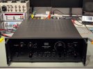
I got this amp in working condition, although with a DC offset of ~50mV, a slightly dirty speaker switch and - only detectable with test equipment - a slightly worse performing left channel.
Someone must have spilled some type of a liquid all over the unit - looked worse in person. Someone had done some maintenance before and replaced some capacitors and resistors, my guess is in the more recent history. They possibly missed the fusible resistors in both the Head Amp and Tone Circuit Boards that were - of course - widely out of spec.

Since replacing a couple of components for maintenance can get somewhat boring, I decided to design three new boards:

Actually, one of the reasons was the smell of the amp, once again. Some people surely like the smell of old electronics, I just don't. That's my excuse anyway.
For the most part I implemented Sansui's original circuit design. A couple of notes though:
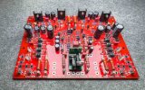
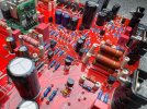
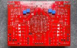
I somehow managed to not take a single photo of either amp module before installing 'em. So these pictures have to suffice:
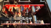
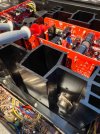
A couple more:
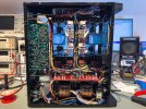
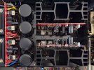
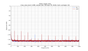
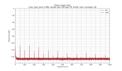
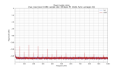
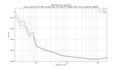
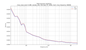
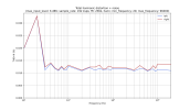
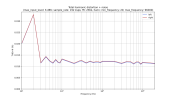
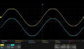
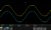
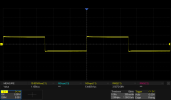
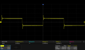
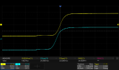
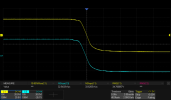
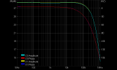
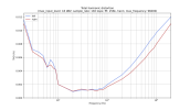
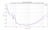
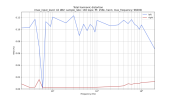
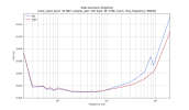
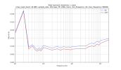
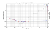
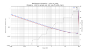
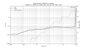
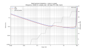
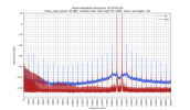
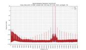
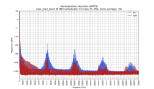
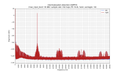
I should be able to provide some before and after measurements soon; I hope for similar (and not necessarily better) results as with the original, given that I replaced all semiconductors, mostly with different types.
If you have any questions, I'm happy to answer.
Sebastian
after having completed a thorough restoration of my Technics SE-9600, now a restoration of my Sansui AU-717 was in order.
I got this amp in working condition, although with a DC offset of ~50mV, a slightly dirty speaker switch and - only detectable with test equipment - a slightly worse performing left channel.
Someone must have spilled some type of a liquid all over the unit - looked worse in person. Someone had done some maintenance before and replaced some capacitors and resistors, my guess is in the more recent history. They possibly missed the fusible resistors in both the Head Amp and Tone Circuit Boards that were - of course - widely out of spec.
Since replacing a couple of components for maintenance can get somewhat boring, I decided to design three new boards:
- F-2663: Power Supply & Protector Circuit Board
- F-2721: Driver Circuit Board (L-CH)
- F-2722: Driver Circuit Board (R-CH)
Actually, one of the reasons was the smell of the amp, once again. Some people surely like the smell of old electronics, I just don't. That's my excuse anyway.
For the most part I implemented Sansui's original circuit design. A couple of notes though:
- I generally favored available modern replacements, where reasonable.
- Tweaked some of the component values (mostly larger capacitance values for power supply bypass capacitors).
- Use of thermal pads for the thermal interfaces of all transistors; thermal compound only for the interfaces between heatsink parts
- F-2663:
- 2x LM4040 (10V) Precision shunt regulator instead of the 13V Zener diodes in the voltage reference. Totally unnecessary, but functionally it's almost a drop-in replacement except for the resistance values in the feedback voltage divider which I had to re-calculate anyway (see next point). And yes, the voltages seem to be very, very stable - not a lot of thermal drift. Rev B with footprints for both the Zener diode and LM4040.
- Voltage adjustment for pos./neg. regulated supplies with multi-turn pots. Also just for fun. Now both rails of both channels are pretty much exactly +/-33V. Yay

- Use of my solid state relay that I presented here, with a minor additions to the protection circuit (can be easily configured for mechanical relays). For this application with even more robust MOSFETs (IPP022N12NM6AKSA1). This actually reduces the power consumption (and the heat produced by this board) noticeably.
- I increased the resistance of the bleeder resistors. In the original design the resistors get pretty hot and waste a ton of power.
- Used two parallel 3W resistors for the LEDs (2x) to at least drop their surface temperature.
- F-2721/F-2722:
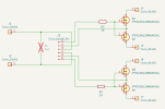
- Two-transistor constant current sinks instead of tail resistors for the JFET diff pairs. Footprint for tail resistor available though.
- Footprints for both the original 2SK97 (DIP-6) and LSK389(A) (SOIC-8)
- One multi-turn potentiometer for DC offset, instead of a single-turn coarse/fine adjustment
- Heat sinks for the VAS transistors (get quite hot in the original design) and pre-drivers (probably not really required at all).
- Driver transistors do NOT use the tab, instead the collector lead is used. Would require modification to use the original drivers with the cut collector lead. I do not like Sansui's approach from a mechanical standpoint, although it simplified the board layout, so it made sense back then. I do not have to worry about that as much with two layers available.
- Re-used the original 2SK97, inductors, driver heat sink
- Footprints for two different options of emitter resistors (original, BPR58 style)
- Rev B with different mounting options for R10, so that both R10 and R04 could probably be mounted on the bottom layer side. Those resistors (3W metal film) get fairly hot (about 80°C for R10) and help those poor (105°C) electrolytic capacitors C02, C04, C11, C14 to dry out faster (measured something like 55°C for C04, so wasn't a huge deal).
I somehow managed to not take a single photo of either amp module before installing 'em. So these pictures have to suffice:
A couple more:
I should be able to provide some before and after measurements soon; I hope for similar (and not necessarily better) results as with the original, given that I replaced all semiconductors, mostly with different types.
If you have any questions, I'm happy to answer.
Sebastian


 I consider publishing it on github once everything is ready (as is, likely under a license that doesn't allow commercial use and forces you to publish your changes/copy left, because then I want all others to profit from those changes too).