• The move to the new server is done. There are some software and database maintenance updates in process. This has us passing the hat around to help out. We appreciate any donations. Seriously, even a dollar helps. The payment page may be found here - https://www.audiokarma.org/support.html

B&K ST-140 RECAP BOM

To JR,
Lets make some further reasoning aling my last post. You said that you applied 70V with the variac. If i take the mains in your country to be 115V, then instead of having +/-62 Volts at the ouput of your power supply, you will have only +/-37.7 V. which is very close to my prototype running at +/-36V. Then my measurements should ve very close to yours.
1-
I adjusted my idle current to 110mA. DC offset adjusted to zero.
2-
Then my R9 (69 ohms) had 1.195 volts across. This is some 17.5 mA. In good agreement with my calculation of 18mA that i mentioned before.
3-
My P2 and its parallel installed resistor combination measures 77 ohms, and i registered a voltage drop of 1.353V across it. Thus 17.5 mA are passing through it. Just as expected.

4-
When i measured the voltage drop across the ends of either of the gate resistors (1000 ohms each) i get zero volts, thus no gate current. Again this is to be expected at idle.

Q9 and q10 get barely warm. nothing to worry about.
You can try to bring down the idle current to 110mA and do these measurements and compare to my values.
Just as a point of note, my mains from the wall averages about 119 V, often as high as 121. Stay tuned.

jrh
 
between 125-131 here...got several stepdown transformers, timers, surge protectors, filters for the appliances.....
 
Hey guys, ST 140 update here.
Testing the right board again had the identical result. Just as I hit 90 VAC on the variac, she let loose. Burned out R9, wasted Q9 and Q10. All other components seem to test fine after the burn out. I've studied your comments jose, and mostly follow them. I appreciate the approach, and will implement as appropriate to the situation. Given the way things present here on the ground,since it happens so suddenly, and at such a precise power input, I'm suspecting the K135 output MOSFET. I want to test the idea that even though the transistor tests good on my tester, it may be failing with the application of higher voltage. Wouldn't be the first time.

I've replaced the smoked components, and am going to try again with the new output transistors in place instead of the new old stock Hitachi's. We'll see how it goes. In the interim, I've been working on a few housekeeping chores on the amp, so lots to do.

I'll keep you posted. Thanks for the help.

jrh
 
The idle current depends on the rail voltages. By all means test the 2sk135 and make sure it is ok.
But you may try adjusting the amp at 70 or 100 ma of idle current. Then set the dc offset to zero and leave it powered for a while to see if anything overheats.
I know b&k specified 200mA, but if you reach the 200mA of idle current at 70v of the applied mains with the variac, as soon as you increase the voltage your current will increase. That is why i believe that you should leave the idle current at less than 200mA when your variac applies 70V. May be set it to some 70 or 100mA at 70 volts and then after you know that nothing overheats, increase the voltage without adjusting P2, while monitoring the current. If the current overcomes 200ma back P2 a touch to remain below that threshold. if you manage to apply your 120V and the unit stays ok, then you are done.
But as long as nothing overheats and your dc offset is close to zero mV, there is no harm in using 50mA or 100mA. Only the crossover distortion will be larger than specified.
 
Hey jose, thanks for the thoughts. In keeping with your reasoning, I had the same thoughts, continuing to adjust the bias to well below 200mA at the 70 VAC mark on the variac. When the board ran away at 90 VAC, the bias current was reading at right around 100 mA. It seems to be triggered by exceeding a threshold rail voltage. That's why I suspect K135. I've seen transistors before that test fine at lower voltages, but still fail at real world voltages. The next power up should test that. I almost hope it fails again, because if it doesn't, it probably means my $16 each NOS Hitachi's are flawed. :)

I'll let you guys know how it plays out. Got anymore popcorn ray? :)

jrh
 
Reading your lasts posts i got realy concerned about Q9 and q10 burned during your test. I worry about those and may be the piwer mosfets being fakes. Where did you buy these parts? . Can you post pictures of your 2sk135? I want to compare with the ones i have to see if i spot anything suspicious.
I have read a lot lately about this amplifier, and frankly i got the impression that the 2sk135/2sj50 mosfets are very tough. Aparently is hard to ruin them, so i am becoming more skeptical about the NOS power mosfets that you have.
You had no problems using the buz900/buz905, mosfets, so think your idea of going back to them is a good plan. Eventually, if you need new output mosfeys, there are other lateral mosfets currently made by Exicon from a reliable supplier in the uk.
But those BUZ mosfets are supposed to be very good.
 
yes, Jose' es maravilloso! :trebon:
I traced those BUZZ mosfets to a British company...emailed them to verify. wouldn't trust transistors sold on the bay, unless it's a local company with a history.
 
Reading your lasts posts i got realy concerned about Q9 and q10 burned during your test. I worry about those and may be the piwer mosfets being fakes. Where did you buy these parts? . Can you post pictures of your 2sk135? I want to compare with the ones i have to see if i spot anything suspicious.
I have read a lot lately about this amplifier, and frankly i got the impression that the 2sk135/2sj50 mosfets are very tough. Aparently is hard to ruin them, so i am becoming more skeptical about the NOS power mosfets that you have.
You had no problems using the buz900/buz905, mosfets, so think your idea of going back to them is a good plan. Eventually, if you need new output mosfeys, there are other lateral mosfets currently made by Exicon from a reliable supplier in the uk.
But those BUZ mosfets are supposed to be very good.
Hey jose,
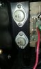
I too have begun to question the output MOSFETs. I've attached a picture of the two suspects sitting in the penalty box. They do not appear to be fakes to my eye, but as I have said earlier in the thread, anything purchased off of ebay has to be guilty until proven innocent. At any rate, just to recap, the left side board dialed in fine with the NOS transistors. So at least that pair is working fine. All four test good on the transistor tester, which sources about 3V DC during a test.

In the process of reviewing my procedures, I realized I may have made a bone head mistake, so I pose a hypothetical question: Assuming I was not monitoring the DC offset, ahem, "correctly", could a high DC offset cause the surge in current that I experienced? I don't think so, but I wanted to get your take on that. In any case I've got the BUZ trannies installed, and will give it another go. Thanks for the input.

jrh
 

Attachments

what I have... look exactly like the ones another AK member at the beginning of this thread has.
 

Attachments

  • 20201015_175009.jpg
    20201015_175009.jpg
    81.9 KB · Views: 31
Last edited:
Hello @JR Harley and @raycarr00,
Hard to tell. They look similar to my 2sk134 and 2sj49. But mine do not say japan on the j49. Only the k134 says japan. Mine do not have bold letters for. the part number and logo. I bought them in Bangkok, in a shop, they may be fakes, also.
Ray's mosfets look a lot more real... So really i. am not sure if yours and. kine are fakes or just fine..

If i remember correctly you were able to reach full voltage with your buz900/5 pair. If so, it is a good idea to go back to those.
Now the 2n3440 and 2n5416 are 1 amp transistors, so i am surprises they got fried also. Are those from. ebay also?

The large dc offset may be causing you problems with the idle current if you have a large DC offset and a load at the output.
Wheb you said that you were not monitoring the offset correctly; what did you mean exacltly?
 
Hey jose,
One of the first things I did when I received those NOS parts , was to compare them against the original factory output transistors. They are identical. I even examined them under the microscope to look for any manufacturing discrepencies. I'm 99.999% confident that they're legit. That doesn't mean they're good though. 40 years old right? And you can't tell if they're pulls, because they're socketed, not soldered in. Q9 and Q10 were sourced from Mouser.

Embarassingly, I'm thinking that perhaps on the last test, I had the probes from the meter measuring DC offset on the left side output, and not the right! Which means whatever I was measuring was meaningless, but I can't be sure. DOH! I've now learned I should take a picture of my test setup after any failure. Since I took everything down, I can't say that's what I did, but it could be a possibility. I'll power up with the new components and see what happens. Stay tuned.

jrh
 
I have made much worse mistakes than that!. Lets see what do you get when you power it up. Write down the dc offset and the idle current and the rail voltages against ground. I am intetested to know If you are able to adjust the biad ans offset.
 
ST-140 fan boys, ............update here.
Hope everyone is well.

So I have GOOD NEWS! I burned up R9 again, and if experience is any guide, Q9 & Q10 as well. The good news is, that it does seem to rule out the output trannies as a suspect, since I was using the BUZ MOSFETs this time. As in the previous two attempts, right at 90VAC, R9 let out the magic smoke. I have another curious situation here apparently.

The left side board adjusted fine, and it is identical to the right side. Strange. I think I'll re-test the left side under the same conditions again, to see if I can learn anything from that.

One curious thing I noted this time: With zero voltage in from the variac, the meter monitoring the DC offset from the speaker terminals, read 157mV. Why wouldn't it read near zero? I suppose the caps could be discharging and presenting that kind of value at the speaker terminals, but it just seemed odd.

I'll re-do the right board again, dust myself off, and get back to it. I'll report back on what the left board does.

jrh
 
iHi RJ,
The set R9-Q9-q10 blew in only the right channel?
That is a good hint.
I saw in one of your pdf files that one of the gate resistors in that chanel is different from the others. You can see this in the pdf file you uploaded on page 3, post #45. Look at the 4 gate resistors. Are all the same and 1K ohms?


The dc offset when the unit is turned off is not zero because the capacitors c5, c5 c6 and c7 hold charge. I experienced this in my pdototype as well. Before i power the amp to test i always discharge these caps by momentarily shorting them. Then the dc offset goes to zero. I also discharge the main power supply capacitors every time for safery reasons. I do this with a 24V filament lamp which is rated at several amps.
 
No drama on the left side guys. The left side board, with the NOS output MOSFETs still installed, comes up in a very reasonable way at 115VAC. The components are obviously warm and workin', but not HOT, like the right side. I feel like I'm narrowing things down at least. Something is definately wrong on the right board. The frustrating thing is, it looks like it's built just like the left side. More study is needed I suppose. Stay tuned.

jrh
 
iHi RJ,
The set R9-Q9-q10 blew in only the right channel?
That is a good hint.
I saw in one of your pdf files that one of the gate resistors in that chanel is different from the others. You can see this in the pdf file you uploaded on page 3, post #45. Look at the 4 gate resistors. Are all the same and 1K ohms?


The dc offset when the unit is turned off is not zero because the capacitors c5, c5 c6 and c7 hold charge. I experienced this in my pdototype as well. Before i power the amp to test i always discharge these caps by momentarily shorting them. Then the dc offset goes to zero. I also discharge the main power supply capacitors every time for safery reasons. I do this with a 24V filament lamp which is rated at several amps.
Hey jose,
Yes, those resistors all read 1K "on the dot" prior to the test. I'll check them again. Most of them I had replaced, that's why one looks different. But something is letting too much current flow. Makes sense that the caps still had a little charge in them causing the DC voltage at the outputs, it would be the only possible source I suppose. I'm currently doing triage on the right board components. When I get it re-built, I'll go from there, probably do something like you suggested and test some circuit voltages under low power, say 30VAC. I need more meters! :)

jrh
 
ST-140 right board forensic exam report here:

Yes, it appears that Q9 & Q10 are wasted once again. I find I am growing weary of replacing $3 transistors on this circuit!

In looking at the schematic, I decided to test the LED associated with R7, as well as R7 itself. The LED is testing bad. It's showing a .237 V drop across each side. That is not right. Should be a .6V drop across one side only. So something is hinky there. Left side board LED tests correctly. I think I have a suitable replacement, but I'm not 100% sure what that little red bastard is actually doing anyway! It's clearly a part of the biasing circuit, so I'll replace it and see where it goes. Maybe you can shed some light on it jose. At any rate, the journey continues. I'll likely have to pull R7 to test it, it's reading all over the place. Take care all.

jrh
 
Back
Top Bottom