• The move to the new server is done. There are some software and database maintenance updates in process. This has us passing the hat around to help out. We appreciate any donations. Seriously, even a dollar helps. The payment page may be found here - https://www.audiokarma.org/support.html

Crown D150A - Puzzled. Fixed itself, then distortion came back. DC offset.

I'll zoom on them tomorrow. BTW, having -5V where the schematic calls for +1.75 is not OK.

I think you need to test the unit at full voltage to get reliable readings.

Please test with full voltage and write down some voltages, at least from the input to the R206 - R207- Q200- Q201 -R216 network.

If you can, use the full schematic, there are parts not visible in this crop. Writing in only 1 channel is OK, you can write voltages for both channels on one half of the schematic, so they show larger. Numbers show a bit small in my computer.

Check if you can download this image. I can send you a higher resolution file if you need.
https://drive.google.com/file/d/1oQvuP3sSdWQrOnHrcRZn_vCcIig02lHm/view?usp=sharing
 
Will do - I'll switch off the DBT and test voltages at full power.

Thank you for the schematic, I do have that whole schematic in my file with voltages recorded for the whole circuit, I just can't post it here at high enough resolution that you can read it. It would be too small. I'm trying to figure out how to share it. Will get readings at full power first.
 
Plugged into the wall and the voltages shifted a bit. The IC pin readings seem normal (note that Pins 1 and 13 don't match the schematic, but they match each other as well as another good D150A I have), but I'm seeing around -250mV to -350mV on Channel 2's output (it fluctuates a bit), and the IOD light is on.

Full power voltage readings taken and recorded into my powerpoint, then saved as a PDF. The PDF is attached to this post. (Colors: green is good channel, yellow is bad channel); "#####" just means I haven't measured it yet.

The most obvious issue is Q212. It gets VERY hot, and the collector voltage is about 6V too high. However I've verified over and over that Q212 is good (the original SS7304), as is Q213 (original 2N3585) and Q214 (original 2N5631). Plus, Q213 emitter / Q214 base voltage seems fine. So - why would excessive current be flowing through Q212? Maybe a shorted D207 (which is a good new diode)? Other ideas?
 

Attachments

Last edited:
Well done ! we are getting something !

Something is definitely wrong at Q212, collector voltage is way off, plus excessive heating. Check everything in that network, including Q211 and Q213. You have a very high voltage drop at Q213 Base to Emitter (if that's not a typo). A good transistor should read about 0.6 - 0.7 V from base to emitter. Measuring the voltage drop across resistors connected to a transistor can tell you if a transistor is conducting or not. Perhaps Q213 is not conducting as it should and Q211 is holding all the voltage (just guessing, but possible). It's also possible a broken solder , or bad connection between Q212 and Q213.

Also, you wrote -44.1V at Q205 base, and -43.8 at Q201 collector. Those points are electrically connected, they should measure the same. 0.3 volt is not too much, it could be just the measurement tolerance, but just in case, check continuity between those points. It's possible you have some poor soldering, or broken pcb trace dropping 0.3V.

A transistor backwards can be the cause too. So , check every transistor you had replaced, if in doubt post it here. Check with your DMM in diode mode. The lead with higher voltage drop from the Base, should be the emitter. I've seen same part numbers with different pinout (probably different manufacturers or fake parts). Also, a transistor can test good at the DMM, and fail under the higher voltage in circuit.

Can you adjust the "good" channel DC offset?
 
Last edited:
Thank you!! Spent some time on it today - Not out of the woods, but a step in the right direction after scrutinizing my orientations.

It turns out, I got my pin orientation backwards when hooking Q213 back up. I had Q213 B and E swapped. So you were right on @elnaldo about Q213 not conducting like it should!

My other replacement transistor orientations are good:

Q203: Using KSC1845 (ECB) in place of 2N3859 (EBC)
Q205: Using 2N5551 (EBC) in place of MPSL01 (EBC)
Q208: Using 2N3905 (EBC) in place of 2N4125 (EBC)

But now ... I have -1.0V at Channel 2's output. This time, I can't see any smoking guns. Can you? Check out the new measurements.

Note that the DC offset, at first power-up, starts at -0.7V and then steadily falls to around -1.0V. If I blow on the circuit board, it rises a bit, but never back to 0. The IOD light stays illuminated. Also, note the op amp's pin 8. On powerup it starts around -35mV, and falls slowly to around -48mV. This seems to track the slowly falling DC offset value as well ... huh.

To answer the last question, yes, I can adjust Channel 1's DC offset to 0.0mV, and the IOD light is not on.
 

Attachments

Last edited:
Good news ! As you can see, voltages can tell a lot. Any transistor not having near 0.7V from base to emitter is always suspect, something is happening there.

Did you try to adjust the DC offset now? I see you have +11mV at the left channel OPamp input, but zero at the right channel. perhaps rising that voltage with the adjustments can correct the DC at the output.

Also, if you replaced transistors, you should check the Bias adjustment (R228). You can fit a trimpot to adjust it, and then replace with a fixed resistor of the right value.

I see something is not OK around Q202, Q207. I'd check a bit around R210, Q202, Q2027, Q206 to see what's happening. Perhaps Q202 not conducting as it should. I understand Q202 should bias Q207. But perhaps the DC ajustment corrects all this.

Also, Q203 plays a role in there, and I see you have used a KSC1845 (a 50mA part) to replace the 2N3859 (a 500mA part).The manufacturer for sure have used a 500mA part for a reason. Perhaps the 2N5551 is a better replacement for the 2N3859 (I don't know the data you checked to use the KSC1845)
 
Last edited:
Back to the D150A.

First about the replacement transistors.

  • I have 2N3905 in place of 2N4125 at both Q208 and Q108.
  • I have 2N5551 in place of MPSL01 at both Q205 and Q105.
  • I have KSC1845 in place of 2N3859 at only Q103 (it was at Q203 on the bad channel, Channel 2, but I swapped it with the good 2N3859 at Q103, and there's been no change in my voltages). Therefore, believe it's conclusive that the KSC1845 replacement has no ill effects on the circuit.
  • At Q202 and Q207, I original parts at both that I swapped with the other channel earlier, with no change. So I'm inclined to think Q202 and Q207 are OK but will continue to investigate related components as you mention @elnaldo .

Second about the adjustment pots.

  • R202 does nothing to adjust the DC offset.
  • R200 does something, but not much. It can adjust the DC offset from -0.8V to -1.1V.

Third about new observations.

While measuring, I also measured more values around the op amp inputs and found something very interesting.

On the good channel (Channel 1) I am seeing 1.4V across R104; this is the resistor between the output adjustment pot R100 and pin 6, Channel 1's op amp inverting input. I'm seeing -1.4V at R100's output; Pin 6 measures 0mV.

On the bad channel (Channel 2) I am seeing 6mV across R204! I'm seeing -54mV at R200's output; Channel 2s op amp inverting input, pin 8, measures -46mV.

That's a huge difference! I am trying to see how I can figure out if it's a symptom of the problem, or the source of the problem.

I've attached updated circuit diagram measurements.
 

Attachments

Last edited:
Hello.
The fact that R202 does nothing, makes me think in that network. You should have 5V across R202 external pins, same at R102, and a variable voltage at the middle pin, it should move from 0 to 5V depending of the trimpot rotation.

Then, of course that voltage should be connected (continuity) from R202 center pin to R201-R203-PIN 9 on the IC. Please check all that network has continuity, resolder and check all those resistors just in case.

Also, check voltage across R100 and R200. They should match. Also resistance value, check both resistors are within specs.

Also check the volume pot and associated wiring, ground connections. Just in case. A problem there could cause a small DC offset.
 
Thanks @elnaldo ! Investigated, results below.

R102 / R202: Both are OK. Both have 5.9V on them, both trimmers work fine. The voltage drop across R101 / R201 corresponds to whatever voltage is coming from the trimmer, dropping it to 0.0mV at R103 / R203 regardless of the position of R102 / R202 trimmers.

R100 / R200: Both are OK (both are actually new single-turn Bournes), both have correct +/- 10V on either side and they match. I realize I had a brain fart previously - R200 works fine, it's not stuck at -54mV. I adjusted it to match the other channel, so there is -1.4V at R204. However, this did not significantly change the -48mV at Pin 8. It's the same with the other channel, i.e., adjusting R100 does not change the voltage at Pin 6 by more than 1mV.

R105 / R205: Both are OK. No DC offset coming in from input / gain pots.

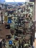
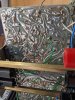
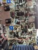
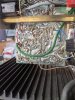
I've attached updated measurements, and I'll also put up some pictures since pictures can sometimes help grease the skids when solving problems.

Good channel 1:

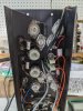
PXL_20210110_213425755.jpg

PXL_20210110_213727906.jpg

Bad channel 2:

PXL_20210110_213421399.jpg

PXL_20210110_213731665.jpg

The outputs / drivers (that's the IOC board draped over the side):

PXL_20210110_213436923.jpg
 

Attachments

Update on this ... I found that C203 had 0.5V across it, and when I measured it with my multimeter the IOD would turn off. A great clue, I was that much closer to figuring it out.

AND THEN

I barely slipped with the multimeter lead :eek: and the next PCB trace over has 45V on it. :mad: ZAP!... I think ZAP. Not sure what happened yet.

But something happened ... Now the IOD light is OFF, but I am seeing -4V at each output.

Time to start the diagnosis from scratch.
 
Last edited:
For anyone following along, it looks like the negative zener in the IC circuit let go. It's building less than 1V across it and measures shorted.

No other transistors on the board appear to have shorted.

Interestingly C203 measures a correct 200pF.

I'll need to order a bag of 10V 0.5W zeners and let's see how things look once I've got a working D5 again.
 
With the new 10V zener diode in for the IC's -10V power supply, strange results.

I'm now seeing -0.4V DC offset on both channels!

I'll start measuring - again - starting at the IC pins and working through the channels from there.

Edit: First measurement is across the new zener diode. It's only developing 8.5V instead of the rated 10V. Does this mean it's defective? Or perhaps I ordered too large a zener and am not giving it enough current?

Hmm ... looking at the datasheets.

Original: 1N961B
Vz = 10V
Iz = 12.5mA

Replacement: 1N5240B
Vz = 10V
Iz = 20mA

I need to see if I can calculate or measure the actual zener current in the circuit. I suppose if it's only 12.5mA, then I can't expect to see 10V develop across the 1N5240B.
 
Last edited:
Doing a quick calculation, R8 drops from -45V to -10V. A drop of 35V across 2.7K is about 13mA.

So, I don't think the circuit puts 20mA through the zener.

I'll put this BACK on the shelf and add as close to a 12mA Iz part as I can find to my next Mouser order.

Unless - can someone confirm I'm thinking about this correctly? Or am I wrong about this?
 
Last edited:
Aside from your accidental mishap and shotgun troubleshooting, I still think it is something simple like dirty switches or cold solder joints or some such thing somewhere because when something works and then has an intermittent problem, it is usually not a bad part. I know these types of problems can drive a person crazy.
 
Thanks, what do you think I should do, if it's not a switch or solder joint issue? I'm trying to figure out how my steps at diagnosis were shotgun troubleshooting, and if so, and if you mean that in a bad way, what can I do to improve my method?
 
Any update ? - doing similar diagnosis on a Crown D-150 with blown Q105 and Q106 - just waiting for replacements. I have a horrible feeling my problems will not be solved by replacing those.
 
@Simon H I've actually recently put this back on my bench ... so far, no breakthroughs. I'm still seeing ~ -0.5V in each channel (little higher in one channel).

I replaced the two remaining (making 3 total replaced) 10V zener diodes for giggles, but it didn't change anything.

I've measured the voltages (again) through the pre-driver / driver / output stages, finding they all are operating correctly.

So ... short answer, no update but I'm actively working on it again.
 
Good to hear. Mine is working again. Anything in the feedback loop screws up the output of the op amp. I actually blew something and got 45v offset on both channels which flummoxed me until I realised the mono switch was set. This joins both feed back circuits. The trimmer pots have the wrong numbers in the manual. On the schematic they are r100 and r102, not r103 and r105. 12voltvids, YouTuber got flummoxed with a crown amp with a massive dc offset on one channel. Interesting watching him go through his diagnostic steps. Basically any component can push it out of spec. You’ve checked all you semiconductors. I put mine through a cheap component tester and got lucky.
 
Thanks @Simon H for the tip about 12voltvids (he has a couple videos of a DC300 diagnosis, if that's what you meant). It was really interesting to see his thought process in diagnosing it. That's the kind of thing I'd love guidance about here ... like, how should I be thinking about this?

Seems like the DC300 has a similar circuit to the D150A, so his thoughts about the opamp and the feedback circuit was really interesting.

Unfortunately my opamp seems OK, my zeners are new already, and none of the transistors appear to shorted ...

Great tip on the mono switch tying the feedback loops together. Having -0.5V DC on both channels is weird. Maybe that has something to do with it.
 
Back
Top Bottom