Will check it again tomorrow. I did check C11 and there is no voltage across the pins.Let's go down the list:
- "Fuses have continuity." -- Good
- "C3 and C4 measuring 23.5v DC." -- Good
- "When measuring IC1 and Q5 I use DC with black lead to chassis correct?" -- Yes, black to chassis. Pin 1 = Input, Pin 2 = Output, Pin 3 = GND (chassis)
- View attachment 3006244
- "When measuring C11 I measure dc red to + and blk to - correct?" -- Yes, red to (+) black to (-). This should be the same as the regulator (IC1) output voltage, 12.1VDC.
- "Still no readings from the transistors with bk to chassis ground and using + probe to transistor legs." --
- Pin 2 of IC1 (previous measurement was 21V) should be the same as C11 (+) and Q5 collector?
- If not, look for a break in the PCB trace. You can turn off power and use ohms to check continuity from IC1, pin 2 (see diagram above) to C11 (+), to Q5 collector.


You are using an out of date browser. It may not display this or other websites correctly.
You should upgrade or use an alternative browser.
You should upgrade or use an alternative browser.
Harman Kardon CD491
- Thread starter vegas79
- Start date

Please verify the voltage on IC1 pin 2 to ground (pin 3 should also be ground).
Here is the path from IC1 output Pin 2 to Q5 collector (Magenta line).
With power OFF, please verify with an Ohm meter that you have continuity from IC1 pin 2 to Q5 collector.
Follow the trace continuity through the two jumper wires all the way to Q5. You should have close to 0 ohms at the two jumpers and at Q5 collector.
If there is no continuity, then inspect the solder joints of the two jumper wires, IC1, and Q5 collector (middle pad).
With power turned-on, you should have close to 12V at IC1 and at the two jumpers, and Q5 collector.
Thanks.
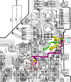
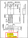
Here is the path from IC1 output Pin 2 to Q5 collector (Magenta line).
With power OFF, please verify with an Ohm meter that you have continuity from IC1 pin 2 to Q5 collector.
Follow the trace continuity through the two jumper wires all the way to Q5. You should have close to 0 ohms at the two jumpers and at Q5 collector.
If there is no continuity, then inspect the solder joints of the two jumper wires, IC1, and Q5 collector (middle pad).
With power turned-on, you should have close to 12V at IC1 and at the two jumpers, and Q5 collector.
Thanks.
Last edited:
I have continuity from Q5 collector right up to the trace pad with the open unused thru hole. When I check continuity from Pin 2 to Q5 Collector I have zero. Should that trace pad (with hole) possibly be soldered to Pin 2 on IC1? If it was soldered I would then have continuity from IC1 to collector of Q5.Damn now I have gone and done it. While rechecking voltage at pin 2 on IC1 my probe slipped and I got a spark. Now Zero voltage at pin 2. I may shorted IC1. On the rare positive side I may have found a broken trace Q5
Any suggestion on a replacement for the IC1 I have apparently shorted?I have continuity from Q5 collector right up to the trace pad with the open unused thru hole. When I check continuity from Pin 2 to Q5 Collector I have zero. Should that trace pad (with hole) possibly be soldered to Pin 2 on IC1? If it was soldered I would then have continuity from IC1 to collector of Q5.
I have continuity from Q5 collector right up to the trace pad with the open unused thru hole. When I check continuity from Pin 2 to Q5 Collector I have zero. Should that trace pad (with hole) possibly be soldered to Pin 2 on IC1? If it was soldered I would then have continuity from IC1 to collector of Q5.
Attachments
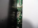
OK. Here's what I think is going on (see photo and board layout).

- I flipped the board layout from the SM so I can read it from the back to match your photo.
- Tried to match up solder pads between the two.
- The turquoise blue lines and dots are IC1, regulator.
- Looks like whoever soldered the IC1 put it in the wrong holes!!! It should be moved down one hole.
- You should be able to check continuity from the open hole to C9.
- Now the question is: Is there a jumper installed as shown by the light orange line?
- Also, in the photo there is an additional solder pad (red square) that is not in the layout. Is there anything soldered to it on the top side of the board?
Last edited:

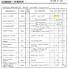

Holy Smokes! I think you may have found the main source of the problem. Its all starting to make sense now as I finally got in touch with the old friend who gave me this "nightmare". I pointed out that he had told me this had worked great but had quit working. He now tells me it worked great until after he got it back from the rebuild. He was in the process of moving out west when he got it back from repairs and never followed up with the person who did the rebuild. Yes there is a brown jumper indicated by your diagram. The orange pad you speak of is a blank one with a dab of solder on it from the factory. I just unsoldered the lugs of the IC1 and he had one of the lugs soldered to one end of where the jumper wire goes thru board! The whole IC needs to be shifted down which will solve the continuity break between Pin 2 and Q5. You folks are Amazing. I would have never caught that. Now I have to order some parts such as the voltage regulator. I wonder what else shorted with that regulator in the wrong spot such as Q5. I don't mind ordering a few things that may be questionable R20 and R27 are on the way already. I may order some 470ohm Nichicon caps to replace those three Fine Gold ones that are installed and maybe the 4700 Fine Gold as well.
We'll see if anything else was damaged with that part inserted incorrectly. Since the regulator is <$1.00 I would order several, just in case we burn out one while troubleshooting other things on the board.
For power supplies, I have been using Nichicon UPW series. They are temperature rated to +105C. Digikey usually stocks them.
Just checked, they have the 4700uF in stock... you can check the others.
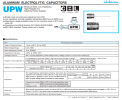
For power supplies, I have been using Nichicon UPW series. They are temperature rated to +105C. Digikey usually stocks them.
Just checked, they have the 4700uF in stock... you can check the others.
Replacing IC1 should take care of all of the voltage issues on the upper part of the schematic. There is one issue on the lower part, Q4 and D5 Zener.
You previously measured the emitter voltage of Q4 to be -20.9v and it looks like it should be -4.7v. Double check this. You can order a spare Q4 and D5 Zener to replace if needed.
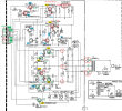
You previously measured the emitter voltage of Q4 to be -20.9v and it looks like it should be -4.7v. Double check this. You can order a spare Q4 and D5 Zener to replace if needed.
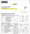
Q4 shows as a 2SA1115F or 2SA1115E. Any suggestions for a replacement in case its faulty. D5 is a RD9, IJB2 . Recommended replacement?Replacing IC1 should take care of all of the voltage issues on the upper part of the schematic. There is one issue on the lower part, Q4 and D5 Zener.
You previously measured the emitter voltage of Q4 to be -20.9v and it looks like it should be -4.7v. Double check this. You can order a spare Q4 and D5 Zener to replace if needed.
View attachment 3006587
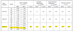


genesmasher
Active Member
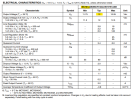
Make sure the board is in fact grounded to chassis (front left screw is attached), if you are attaching your black multimeter lead to chassis. If the board is lifted off the chassis, you will not get correct reading. Transistors I mentioned earlier (KSC2383YTA (NPN) & KSA1013YTA (PNP) ) will work as substitutes for 99% of common transistors used in power supplies. They are rated on at higher (3x on average) voltage/current/power than most obsolete originals. They also have correct pinout (ECB).
Last edited:
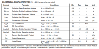
Will either of your recommended transistors be a substitute for the original Q4 transistor (2SA1115)?Make sure the board is in fact grounded to chassis (front left screw is attached), if you are attaching your black multimeter lead to chassis. If the board is lifted off the chassis, you will not get correct reading. Transistors I mentioned earlier (KSC2383YTA (NPN) & KSA1013YTA (PNP) ) will work as substitutes for 99% of common transistors used in power supplies. They are rated on at higher (3x on average) voltage/current/power than most obsolete originals. They also have correct pinout (ECB).
Those KSA733C's are NLA from Digikey and Mouser.??? See my previous post #153.
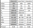
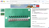
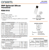
Try these KSA1015YTA from AK member @EastPoint, excellent supplier, or Mouser & Digikey also have them.
genesmasher
Active Member
Last edited: