• The move to the new server is done. There are some software and database maintenance updates in process. This has us passing the hat around to help out. We appreciate any donations. Seriously, even a dollar helps. The payment page may be found here - https://www.audiokarma.org/support.html

Marantz 2275 rebuild

I digitized PE01 from original board that i have. And then Made layout of elements from the manual.
I am going to use it as reference to reproduce correct schematic and new PCB.
Schematic that we all have in our manual is wrong
 

Attachments

  • elements.png
    elements.png
    251.2 KB · Views: 23
  • traces.png
    traces.png
    130.9 KB · Views: 23
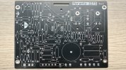
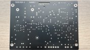
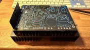
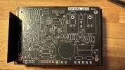
Finally P700 arrived this morning.
I am going to do a trace check again to make sure its ok. Btw they are also design for Marantz 140. Since pcb is essentially the same.

Also i did pcbs a bit bigger in height than original for better laylout. Will see if it could be an issue, but my modeling showed it shouldn’t
 

Attachments

  • IMG_7985.jpeg
    IMG_7985.jpeg
    128.1 KB · Views: 31
  • IMG_7986.jpeg
    IMG_7986.jpeg
    87.6 KB · Views: 30
Moving resistors is very tedious process. I have checked their nominals when i did schematic. Check was done by measuring each individually.

Now i desolder one, put on to new pcb. One by one. Then i do check agaist the list that nominal matches.

Moat of the resistor arr ok, but i have checged some of them.

R716/717: they are supply. Originally 1.5W. But they were very hot when i did load testing. Replasin them with 2W. [CPF21K5000FKE14]

R718/719: replaced to precise one with low ppm 680 0.1% 15 PPM [RN60D6800FB14]

R725/726/736/737: 100R 0.1% 1/4W 15 PPM [H8100RBYA]
 

Attachments

  • IMG_7993.jpeg
    IMG_7993.jpeg
    152.1 KB · Views: 34
Slowly going to the end. H709 is replaced and it doesn’t have metal back, so i can achieve better thermal coupling with H713. But there is a clearance now so i need a spacer. Will figure something out.
 

Attachments

  • IMG_7996.jpeg
    IMG_7996.jpeg
    143.5 KB · Views: 33
  • IMG_7995.jpeg
    IMG_7995.jpeg
    149.9 KB · Views: 33
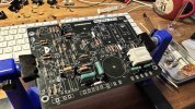
I just soldered it and plugged in. No transistors replaced except mentioned above. Relay seem to click. There is noise when i put full volume (as it was before). Waiting till it will get hot to adjust bias
 
I am amazed. It worked! Everything was able to adjust to the required level. DC offset is 0mv. Bias 10mv. It is so nice to adjust with multi turn pots.
Now when I am certain that layout is correct (evidence based approach, otherwise it wouldn't play the sound) i will replace some transistors and diodes.
Clean the PCB and test again.

After that i'll plug it in the audio interface and compare with original one in another channel.
 

Attachments

  • photo_2023-11-24_20-10-28.jpg
    photo_2023-11-24_20-10-28.jpg
    131.4 KB · Views: 33
Looks like you re-designed the board with copper on the component side (or am I missing something). Is there an advantage to doing this? It seems like now you need to rely on plated vias for solder connections and rework runs the risk of breaking the via holes.
 
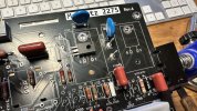
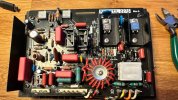
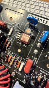
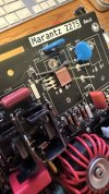
Finally fully assembled with all new components.
Old one is C709 and H711,H712.

Thermal coupling of H709, H710 is done using copper foil 0.1mm to H713.
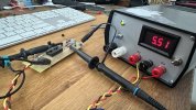
H701/702 was matched using Vbe transistor matcher i build earlier 2 year ago.

I'll post parts list later when I hear this beast will be playing
 

Attachments

  • IMG_8001.jpeg
    IMG_8001.jpeg
    134.9 KB · Views: 40
  • IMG_8002.jpeg
    IMG_8002.jpeg
    114.5 KB · Views: 41
  • IMG_8003.jpeg
    IMG_8003.jpeg
    127.7 KB · Views: 39
Last edited:
WOW!!!!!!!!!!!!!!!

I just joined AudioKarma as I need to rebuild my Marantz 2275 and this is the first thread that I've read!!!!

ABSOLUTELY AWESOME WORK... bitomaxsp!!!! I did download the the Lamp Holder .stl file... THANK YOU, SIR!

 
P700s are assembled and are playing really well. I want to do some measurements, but i have no time.
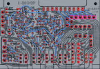
Meanwhile, i am routing PE01. There is nothing to show yet, since original schematic full of error and simply doesn't match the PCB in the amp. So i made trace layout and component layout and reconstructing schematic from original PCB instead. As soon as I have something to show, i'll post it here.
 
Traces obtained by taking picture of the PCBs bottom and cleaning it later with photo editor. Width of the board is 238mm.
 

Attachments

  • traces.png
    traces.png
    130.9 KB · Views: 17
Elements layer obtained from schematic. Cleaned it up a little. As you may notice, it is not in match with traces, but gives good enough understanding of components placement.
 

Attachments

  • elements.png
    elements.png
    251.2 KB · Views: 19
Hi

What footprint did you use for J709 -


I am building a new pre amp and buffer boards for a 1250.
it also has single and double 6 pin and 12 pin pushbuttons.

for the moment I use pads - but I need to position them very precisely - I am using a caliper to measure the exact positions.

I also asked this on the KICAD forum - no answer yet.
 
this is current status:
1742144153450.png

1742144307075.png
I am still adjusting the positions and pad diameters.
the button positions and pin connector are critical as they must fit with other parts.

I tried to underlay the picture of the PCB picture from the service manual - scaling has been a challenge :)

let me know your thoughts/ideas.

Thanks
Robin
 
Hi

What footprint did you use for J709 -


I am building a new pre amp and buffer boards for a 1250.
it also has single and double 6 pin and 12 pin pushbuttons.

for the moment I use pads - but I need to position them very precisely - I am using a caliper to measure the exact positions.

I also asked this on the KICAD forum - no answer yet.
I did J709 myself. If you want, i can share it with you. No a big deal
 
Back
Top Bottom