

You are using an out of date browser. It may not display this or other websites correctly.
You should upgrade or use an alternative browser.
You should upgrade or use an alternative browser.
Need some input on Dim bulb tester behavior
- Thread starter Donguri
- Start date
-
- Tags
- dbt drifting bias hk 560 hk560

elnaldo
Lunatic Member
33mV is not high if the manual calls for 30mV.
Anyway replacing the bias transistor, or swapping the part with the good channel, can help to narrow the problem. Check the components in that network, including the trimpot.
The bias circuit works with the base voltage of the Drivers and output transistors. Any component out of specs in that network can allow a higher current flow raising the bias current.
Anyway replacing the bias transistor, or swapping the part with the good channel, can help to narrow the problem. Check the components in that network, including the trimpot.
The bias circuit works with the base voltage of the Drivers and output transistors. Any component out of specs in that network can allow a higher current flow raising the bias current.
My bad, I ment the bias was rising so fast so I turned it off at 33mV just to be safe, sure it would've continued quite high based on my DBT experience.
Not sure which are the Drivers, is it the Q418 & Q420?
Ok so will try these things then:
-Reheat the worst looking solder joints
-See if I could swap the bias transistors (only reason I´m hesitating is because I've never done it before)
-Replace the trim pot, Got a new Bourns trim pot with the same value.
-Look for bad components.
Btw, Seems like units from this whole line from HK might have Bias issues.
Found this comment on another site on the model over this one
" The 670 has been noted to have reliability and bias-drift problems. (An overbiased 670 can suffer from "thermal runaway.") "
Not sure which are the Drivers, is it the Q418 & Q420?
Ok so will try these things then:
-Reheat the worst looking solder joints
-See if I could swap the bias transistors (only reason I´m hesitating is because I've never done it before)
-Replace the trim pot, Got a new Bourns trim pot with the same value.
-Look for bad components.
Btw, Seems like units from this whole line from HK might have Bias issues.
Found this comment on another site on the model over this one
" The 670 has been noted to have reliability and bias-drift problems. (An overbiased 670 can suffer from "thermal runaway.") "
elnaldo
Lunatic Member
Q418 and Q420 are the "drivers", they drive the output transistors.
I'd make sure all the soldering and joints are OK in that board, specially where you see a lifted trace or pad. Also, check the bias transistor is properly attached to the heatsink, also check the part number, perhaps somebody replaced it with a wrong part.
Search AK for techniques to repair lifted traces on PCBs . I usually make a kind of "hook" or ring with a resistor or capacitor lead wire, and a longer end soldered to the existing PCB trace (I scrap the green solder mask with some sharp cutter), the "hook" around the component lead.
Then, I'd check again the bias behavior.
If that thermal runaway continues, this pict shows some resistors where you can take measurements that can tell if the transistors are conducting as expected. I mean measure the voltage across the resistors, i.e. DMM probes at each end of the resistor, you want to know what's the voltage drop on that resistor. 0 Volt means it's not conducting electricity. so some transistor is not working . Also, voltage between base and emitter can tell you if a transistor is working as expected. It should be around 0.7V.
If you start to measure inside the unit, keep the DBT , and fix the probes to the test points before powering the unit ON. Reduce the risk of shorting something to ZERO (NO RISK). Anything you see risky, playing with the DMM probes inside the amp, trying to reach some transistor lead while the amp is energized, any dangerous move, don't do it, not even one. It's possible to work with zero risk. Takes longer, but it's safer for you and the amp.
Also, do small steps. A large collection of voltages without sense can be confusing instead of helpful. Start at the output, you already know that at the emitter resistors the voltage is a bit high. OK, check R456 and C420, if you have some voltage across R456, C420 is leaky. A capacitor is an open circuit for the DC, so R456 shouldn't conduct any electricity. Large caps have some leakage but very little. If R456 checks OK, move back and check voltage across R450, and so. move step by step, you can compare with the good channel. If R450 checks OK, you could measure voltage from Q18 base to Q420 base. At some point you'll find something that doesn't make sense or doesn't match the good channel. Something is making the voltage at the emitter resistors to raise. It could be a leaky Q422 or 424 too. I'd expect the voltage across R450 to follow the raising bias. D404 and D406, if leaky at some point, could be creating a current flow at the emitter resistors too.
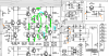
I'd make sure all the soldering and joints are OK in that board, specially where you see a lifted trace or pad. Also, check the bias transistor is properly attached to the heatsink, also check the part number, perhaps somebody replaced it with a wrong part.
Search AK for techniques to repair lifted traces on PCBs . I usually make a kind of "hook" or ring with a resistor or capacitor lead wire, and a longer end soldered to the existing PCB trace (I scrap the green solder mask with some sharp cutter), the "hook" around the component lead.
Then, I'd check again the bias behavior.
If that thermal runaway continues, this pict shows some resistors where you can take measurements that can tell if the transistors are conducting as expected. I mean measure the voltage across the resistors, i.e. DMM probes at each end of the resistor, you want to know what's the voltage drop on that resistor. 0 Volt means it's not conducting electricity. so some transistor is not working . Also, voltage between base and emitter can tell you if a transistor is working as expected. It should be around 0.7V.
If you start to measure inside the unit, keep the DBT , and fix the probes to the test points before powering the unit ON. Reduce the risk of shorting something to ZERO (NO RISK). Anything you see risky, playing with the DMM probes inside the amp, trying to reach some transistor lead while the amp is energized, any dangerous move, don't do it, not even one. It's possible to work with zero risk. Takes longer, but it's safer for you and the amp.
Also, do small steps. A large collection of voltages without sense can be confusing instead of helpful. Start at the output, you already know that at the emitter resistors the voltage is a bit high. OK, check R456 and C420, if you have some voltage across R456, C420 is leaky. A capacitor is an open circuit for the DC, so R456 shouldn't conduct any electricity. Large caps have some leakage but very little. If R456 checks OK, move back and check voltage across R450, and so. move step by step, you can compare with the good channel. If R450 checks OK, you could measure voltage from Q18 base to Q420 base. At some point you'll find something that doesn't make sense or doesn't match the good channel. Something is making the voltage at the emitter resistors to raise. It could be a leaky Q422 or 424 too. I'd expect the voltage across R450 to follow the raising bias. D404 and D406, if leaky at some point, could be creating a current flow at the emitter resistors too.
A wealth of guidance here,
it´s probably worn out phrase by now but Thank you so much for all the details and explanations that makes this frustrating ordeal fun, Hope this comes in handy for others as well.
Will go through the list and do this slowly and safely, going to take a couple of days I think.
it´s probably worn out phrase by now but Thank you so much for all the details and explanations that makes this frustrating ordeal fun, Hope this comes in handy for others as well.
Very basic question but can I use the same assumption for all resistors next in line to Capacitors or is this for C420 particularly? Maybe because it´s next to ground?A capacitor is an open circuit for the DC, so R456 shouldn't conduct any electricity.
Will go through the list and do this slowly and safely, going to take a couple of days I think.
elnaldo
Lunatic Member
All the capacitors are "open circuits" to DC. They block DC. In some tests, I even remove some capacitors because with DC (amplifier idle, not playing music) it's the same a capacitor not present. But you need to know a bit about the function of each capacitor, that's why I can't advice from here to remove some capacitors. But when following a schematic, tracing the DC current flow, read a capacitor like a cut trace, or open circuit to DC. DC won't flow through a capacitor.
In this particular resistor R456, the only way it could conduct electricity is through C420 to ground. But other resistors in circuit can conduct by other paths, just read the schematic and follow or trace current paths from the -V and -V rails to ground.
C420 can be removed or replaced for testing purposes.
BTW, just found this web site, very interesting reading (no affiliation)
http://education.lenardaudio.com/en/12_amps_3.html
In this particular resistor R456, the only way it could conduct electricity is through C420 to ground. But other resistors in circuit can conduct by other paths, just read the schematic and follow or trace current paths from the -V and -V rails to ground.
C420 can be removed or replaced for testing purposes.
BTW, just found this web site, very interesting reading (no affiliation)
http://education.lenardaudio.com/en/12_amps_3.html
Last edited:
elnaldo
Lunatic Member
Perhaps just fixing the soldering solves the issue. Also, measuring resistance between points, with the unit OFF, comparing channels, can reveal a problem. I've found problems that way. Resistance from here to here, comparing channels, until finding a difference (or confirming everything measures the same in both channels)
Hopefully yes, this is my first time reflowing, wonder if a little dab of solder on the iron tip, little drop of flux on the joint and heat at 350C sound adequate for this purpose?
Oh I thought measuring continuity but actually measuring resistance between points? Will add this to the To do-list
Can this reveal bad solder joints as well?
Oh I thought measuring continuity but actually measuring resistance between points? Will add this to the To do-list
Can this reveal bad solder joints as well?
A bit tricky but got the Volt measurements in the end, slow work but good practice indeed.
-Reflowed some of the worst joints, not too skilled at it so didn´t want to go overboard, no change.
-Outputs & bias transistor are original.
-The Bias transistors was attached to heat sink as far as I could determine.
-Checking resistance between joints was a bit confusing so left that practice for now.
Here is a chart over the results, nothing too different between the channels right?
A bit stumped, how could I proceed? Maybe should try to unsolder things?

-Reflowed some of the worst joints, not too skilled at it so didn´t want to go overboard, no change.
-Outputs & bias transistor are original.
-The Bias transistors was attached to heat sink as far as I could determine.
-Checking resistance between joints was a bit confusing so left that practice for now.
Here is a chart over the results, nothing too different between the channels right?
A bit stumped, how could I proceed? Maybe should try to unsolder things?
elnaldo
Lunatic Member
I was reading the voltages, and checking with the schematic. As you see, there is no obvious faults, every resistor shows a similar voltage drop, telling that the transistors are more or less conducting as they should. There are small differences, in some resistors you can see 20 or 30mV differences, and that's significant in a bias circuit, where 30mV is not the same that 50 or 60mV.
In a case like this, I'd start identifying the "undocumented resistor" in the schematic, value and position. Perhaps you need to remove it.
Also, then, replacing the bias transistor Q416, checking VR404 for proper resistance, and It could be that D408 has a higher voltage drop in that channel, making the adjustment range smaller. Is that diode attached to the heat-sink too?
High bias means the voltage between Q418 and Q420 bases is too high and you can't lower it reducing the value of VR404. Check the schematic, follow the transistors arrows, between Q418 and Q420 bases you have 4 "diode voltage drops" (4 emitters), that's approx 2.4V, and any voltage over that will be the voltage you have at the emitter resistors. Then, at the bias diode side, you have 3 "diode voltage drops" at that triple diode, and one more diode voltage drop at Q416, making approx 2.4V too. Between those voltages the circuit finds a balance, adjusted with VR404 due to components tolerances, and Q416 regulating with the heat-sink temperature.
In a case like this, I'd start identifying the "undocumented resistor" in the schematic, value and position. Perhaps you need to remove it.
Also, then, replacing the bias transistor Q416, checking VR404 for proper resistance, and It could be that D408 has a higher voltage drop in that channel, making the adjustment range smaller. Is that diode attached to the heat-sink too?
High bias means the voltage between Q418 and Q420 bases is too high and you can't lower it reducing the value of VR404. Check the schematic, follow the transistors arrows, between Q418 and Q420 bases you have 4 "diode voltage drops" (4 emitters), that's approx 2.4V, and any voltage over that will be the voltage you have at the emitter resistors. Then, at the bias diode side, you have 3 "diode voltage drops" at that triple diode, and one more diode voltage drop at Q416, making approx 2.4V too. Between those voltages the circuit finds a balance, adjusted with VR404 due to components tolerances, and Q416 regulating with the heat-sink temperature.
Appreciate it!
Could the small differences in mV be because of that measurement of both CH wasn't taken at exact same time? I did notice some fluctuation when checking at some points.
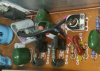
Those trim pots don't seem too healthy. Since I already have new Bourns trim pots at hand wonder if I instead should go ahead and just replace the old ones..
Couldn't find the undocumented resistors in the schematic either. Both channels has them, connected between one leg of the Diode one of the trim pot, both labeled and measures at 10ohm.

Edited to clarify the connected points
Could the small differences in mV be because of that measurement of both CH wasn't taken at exact same time? I did notice some fluctuation when checking at some points.
Not to the big heat-sink but to a heat-sink attached to the Q418:Is that diode attached to the heat-sink too?
Those trim pots don't seem too healthy. Since I already have new Bourns trim pots at hand wonder if I instead should go ahead and just replace the old ones..
Couldn't find the undocumented resistors in the schematic either. Both channels has them, connected between one leg of the Diode one of the trim pot, both labeled and measures at 10ohm.
Edited to clarify the connected points
Last edited:
Am I on the right track with this drawing?
The explanation was great and basic but just wanted to make sure.
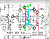
Regarding the Q416, could maybe switch between channels and see.
I did actually order some replacements, searched here on AK for a substitute to 2SC1472K and these two came up:
BC517 (ordered the BC517-D74Z on mouser)
ZTX614
Hope they are appropriate.
One of them has different pin outs so have to study up on that, I'm way over my head here with all of this but got to learn sometime.
The explanation was great and basic but just wanted to make sure.
Regarding the Q416, could maybe switch between channels and see.
I did actually order some replacements, searched here on AK for a substitute to 2SC1472K and these two came up:
BC517 (ordered the BC517-D74Z on mouser)
ZTX614
Hope they are appropriate.
One of them has different pin outs so have to study up on that, I'm way over my head here with all of this but got to learn sometime.
elnaldo
Lunatic Member
What's under that resistor? it should be a cut trace (if the resistor was added between the diode and VR404). If so, it seems it was added in series to the trimpot and diode, to avoid the trimpot to be set at zero. In that case, you could jump the trimpot with a wire, it will simulate the trimpot at minimum position, regardless of any dirty contact or worn carbon trace.
When you say "across" in a circuit like this, I understand it's in parallel with the mentioned device. "across the diode" would be connected at both ends of the diode.
If you feel confident, you can swap Q416 with the other channel. But if you ordered replacements, you could wait and just install the new part.
When you say "across" in a circuit like this, I understand it's in parallel with the mentioned device. "across the diode" would be connected at both ends of the diode.
If you feel confident, you can swap Q416 with the other channel. But if you ordered replacements, you could wait and just install the new part.
Yes that's absolutely correct, it is a cut trace there! Interesting function, is it better to leave it in place then?
Jumping with wire is a foreign concept atm, Wouldn't know where to connect. Will see if I can figure it out.

Have to study up on the lingo.
The order should be in in a couple of days.
Jumping with wire is a foreign concept atm, Wouldn't know where to connect. Will see if I can figure it out.
I can see the mistake I made there, not across rather connected to, pardon, will edit the post to avoid confusion.When you say "across" in a circuit like this, I understand it's in parallel with the mentioned device.
Have to study up on the lingo.
The order should be in in a couple of days.
Some progress!
Replaced the old 2SC1472K (A) with the new BC517-D74Z and the mV dropped from 16mV down to 3mV
It corresponds much better to the trim pot.
It was quite fiddly, had to use long pliers to put it in place and because of the BC517 curved back it had a tendency to turn over to the side (the C1472 was flat), also the BC517 was pinout CBE so had to twist C and B and put an old wire insulator in between to prevent shorts.
New vs old looks like this:
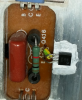

Don't know if something looks way off, like too much compound etc.
The Bias drift might still be present though, will conduct more observations in the coming days so I can't endorse the BC517 fully yet.
But as a first small breakthrough it feels great!
Replaced the old 2SC1472K (A) with the new BC517-D74Z and the mV dropped from 16mV down to 3mV
It corresponds much better to the trim pot.
It was quite fiddly, had to use long pliers to put it in place and because of the BC517 curved back it had a tendency to turn over to the side (the C1472 was flat), also the BC517 was pinout CBE so had to twist C and B and put an old wire insulator in between to prevent shorts.
New vs old looks like this:
Don't know if something looks way off, like too much compound etc.
The Bias drift might still be present though, will conduct more observations in the coming days so I can't endorse the BC517 fully yet.
But as a first small breakthrough it feels great!
elnaldo
Lunatic Member
I know it's not easy, but if you can, only if you can,I think it would be better to have some of the flat sides of the transistor on the heat-sink. The front, or the top. Better heat transfer. It will probably help the circuit to stabilize. Too much compound is OK, original transistors use to be installed with a lot of that grease.
Probably with this new part the bias can be set within specs.
Probably with this new part the bias can be set within specs.
Aaah..OK, it actually is not totally curved, has small flat surface but I see what you mean.
Will see if it´s possible, it would mean crossing all of the leads.
But do you think it will potentially solve drifting?
Short test on full line and was able to dial in to 33mV but with a little initial drift before turning off, tried again through test speakers and both CH sounded fine so far.
A question: Something that was confusing with these transistors (old one and even all of the 4 new) was that all of them read O.L between B-E (red lead on base) has this something to do with because it is a Darlington transistor? Or maybe I screwed up..
Will see if it´s possible, it would mean crossing all of the leads.
But do you think it will potentially solve drifting?
Short test on full line and was able to dial in to 33mV but with a little initial drift before turning off, tried again through test speakers and both CH sounded fine so far.
A question: Something that was confusing with these transistors (old one and even all of the 4 new) was that all of them read O.L between B-E (red lead on base) has this something to do with because it is a Darlington transistor? Or maybe I screwed up..
Last edited:
elnaldo
Lunatic Member
Some drifting is normal, specially if the contact surface is a bit small. The circuit is a kind of "servo" or closed loop circuit, the circuit will be always heating and cooling between a working temperature. That's why better heat transfer from output transistors to the heat-sink, and from heat-sink to the bias transistor, will help to stabilize. I'd think if the bias keeps within the factory spec. and don't start to raise in a thermal runaway, it's OK. Try to monitor the bias for 30 minutes, play some music, check if bias go down again. After 30 minutes the circuit should be stable.
A darlington transistor can read open circuit in some meters, the voltage drop would be 2 times a diode voltage drop, and some meters can't measure that.

A darlington transistor can read open circuit in some meters, the voltage drop would be 2 times a diode voltage drop, and some meters can't measure that.