Chapter 2: The Circuit Board
Geez, where do I begin? I guess my first effort was to identify what this thing was. By every indication, it is a D115 MK I board -- if there is such a thing. The original product was a D115, followed shortly thereafter by the D115 MK II, which was the main line production piece. The original D115 used 6DJ8s in all the small signal positions, and KT77 output tubes. The MK II replaced the KT77s with 6550s (most likely due to the availability of quality tubes at that time), and the driver and cross coupler small signal tubes with 6FQ7s -- an excellent move since the 6DJ8 in the driver position required all manner of protection components around it to deal with the over-voltage conditions (relative to the tube's ratings) that the tube could be subjected to during certain operating conditions. The cross coupler position is a high current position, and was cooking the 6DJ8 there dissipation wise relative to its rating, with both driver and CC positions requiring additional bias resistors to keep the current draw in line. I know the 6DJ8 is a more socially acceptable tube in high society settings relative to the work horse 6FQ7, but in this case, the 6DJ8 is no match for the FQ7's capabilities in these applications, so the move was a very good one. In the MK II, gone are all the protection components and extra bias resistors, making the circuit simpler, and the cross coupling action more effective, even though lower Gm tubes are now in place. The CC position is still a high current position in the circuit (each section passing 10.5 mA), causing each section of the 6FQ7 there to operate at 80% of its Design Maximum plate dissipation rating (based on both sections operating), so that puppy does get hot!
Quick sidebar -- it's interesting that the output tube sockets have all had their pin #1 terminals removed, and there are no facilities on the board to accept a pin #1 terminal were they installed in the sockets. This positively prevents the use of 6CA7/EL34 tubes, which was no doubt the goal of this move since their dissipation rating is lower than that of the KT77 -- a tube that is near universally accepted as a proper replacement for the 6CA7/EL34 --
and visa versa. This points to a significant difference then between the 77 and the other two types: In the KT77, the beam forming suppressor element is tied to the cathode pin (#8) as in 6550/KT88 tubes, where as in the 6CA7/EL34 it is not, but brought out to pin #1. But with no pin #1 present in these tube sockets, those tubes cannot be used then.........
The point of the previous discussion is to say that this board here was designed to support the original design using all 6DJ8 small signal tubes -- but -- it appears to have been factory modified to be a MK II board, as all the protection components for the driver stage are missing (no components were ever installed in those locations), and jumpers have been installed as appropriate (to bypass the original design's extra bias resistors) to configure the board for the MK II design. Since the jumper installations look easy enough to install (and appear to be installed when the board was stuffed), it's unclear whether there was a distinct MK I board and MK II board, or whether there was always just one board, with the MK II amplifiers having the appropriate adjustments made to their boards during stuffing. Either way, my board here is an original design board, but
only partially stuffed with the MK II design components (maaany components missing) -- and is NEW. This board has never seen a millivolt of power applied to it, has never been operationally functional, and has never been installed in a working amplifier. There are far too may components missing for any circuit to operate at all, and where the components are missing, it is obvious to even the visually challenged that no components were ever installed in those locations since the board was manufactured...........in most locations, that is. Finally, this board shows zero discoloration from any exposure heat.
Uniquely (strangely?) however, all the components around the phase inverter tube were originally installed, but then at some point, removed! This design uses a single 6DJ8 as the phase inverter tube for both channels, but all of it's components were stolen in the night. The tube socket itself is present, but only lightly RE-soldered
back in place on just one or two terminals. Now this is interesting. Remember the chassis is for a V70 design,
with balanced inputs. If you remove the phase inverter tube from the D115 design, you could then apply balanced inputs directly to V2 and V3, the push-pull first AF Amplifier stages in each channel. Could
that have been the original intention of the project back in 1990-something? To make a balanced input version of the D115? Of course it never got anywhere near far enough to try it out, so we'll never know for sure.
BUT -- the grid return resistors for V2 and V3 (normally 475K) had 200K resistors installed, which then would have produce the 400K balanced input impedance specified for V type amplifiers and on the rear panel of the V70 chassis. Seems pretty reasonable to me! I mean, who would have intentionally wanted to modify the unit to a balanced input design, when history showed that nobody wanted it? So there's one more piece of the mystery to chew on. Maybe this board was in fact the factory effort to develop a "V" version of the D115, but when sales flat-lined,
that's the real reason the project was scraped. New D115 front panel, new D115 transformers, new D115 board -- never completed and with the previously installed phase inverter components removed, a V type chassis with balanced input provisions to mount it all in, but sales of the concept go nowhere? This picture is really starting to come into focus! Whoever Dr. Frankenstein was however forgot that the heater of the phase inverter tube is wired in series with the heater of V3, so that if you completely remove V1, then V3 won't light and the left channel will be dead. Oops........ Wonder if that's why the phase inverter's tube socket was rather hastily reinstalled, soldered only on the heater pins and one other pin across from them to make for a reasonably secure re-installation...........
But there's so much more -- stuff that just doesn't make any sense. The board itself is fatally flawed in how some of the traces are run around the 3-T regulators (producing a direct short when the proper heat sinks are installed). This explains no doubt why wholly inadequate heat sinks were installed on the 3-T regulators (ones that don't secure to the board), and why the regulators themselves were all beat up with broken leads due to the board being tossed from here to there over the years. One transistor in the bias regulator circuit was actually installed backwards -- and clearly done so when the board was initially stuffed! A jumper was installed to place a dead short across the output of the bias rectifiers (maybe to prevent use of the board since it clearly failed to pass initial inspection?), and other components were of the wrong value by a digit or so (499K installed where a 4.99K should have been, 120Ω installed where 120K should have been, etc.). Also, this board has sockets installed for the IC error amplifiers -- which I'm not sure the production units used. Other components (unrelated to the phase inverter tube) that were originally installed had been removed as if to treat the board as a parts unit -- which it no doubt became in the years after the project stopped, and the unit found its way to the Arkansas audio salon. Heck it may even have been a parts board there as well.
In any event given all the previous information about the chassis and transformers, all of this strongly suggests that:
1. This was a D115 prototype board, produced before actual production boards were run. In pics I've seen of the D115, proper heat sinks were installed for the 3-T regulators, which is simply not possible on this board as designed, so with that, and incorrectly installed components, and incorrect value components installed, the board was likely shelved once the error were found and corrected for the production boards. (Edit: later information now suggests this is in fact a regular production D115 board, with a number of stuffing errors.)
2. During the 90s and the V period of ARC, things were (apparently) pretty lean if not bleak, so it follows that everything was scaled back significantly to keep the lights on. It also follows then that this board could easily have been pulled out of moth balls, and was in the process of being transformed into a V version of the D115 when the plug was pulled.
As a result, and with all the rest of the story that has preceded, the board leaves ARC an absolute mess, with layout errors, only about 60% stuffed, with some wrong components installed and some installed incorrectly, and stuck somewhere in between its intended design, and a V experimental board. No wonder it sat for years with no love. To that point, I have had to correct over
100 points of error on the board -- and I'm not talking about bad solder joints. Everyone of the points was of the type mentioned above, so that the only way to make the board properly operational, was to painstakingly go through it trace by trace, and component by component, so that all the errors were caught. But -- it came with a beautiful chassis, transformer set, and front panel!!

So where does the project stand today?
1. There are 3 boards to this amplifier: the main board, the driver regulator board, and the AC power relay board. The AC power relay board is MIA, so one will need to be made. The driver regulator board is clearly a
similar -- and well used board (heat discoloration showing) -- but not the correct one for a D115. The voltages and terminal markings on the board do not match up with any D115 schematic, but as a regulator board, it is similar enough that it can be properly modified to do the job, as otherwise, it fits in place perfectly. That has been done and tested, so it is good to go. The main board has had all of its issues resolved, and has even had all of it's power supply and small signal circuits tested and proved out now, so that the output stages are the only elements of the board un-powered, and untested. But they have been thoroughly examined and verified to be without fault, although no tubes have been installed yet for operational verification. I did take the opportunity however to replace the insanely large (2W) screen and cathode resistors with appropriately sized components -- 0.5 watt cathode resistors, and 0.25 watt screen resistors (now 100Ω each). These resistor ratings will still allow the amplifier to produce full power output all day long if desired. Apparently, ARC amplifiers are somewhat known for these resistors blowing out -- and sometimes spectacularly so. Using the correctly sized components will minimize any damage done should this happen (sometimes burning a hole in the board!!). Increasing the screen stoppers from 47Ω to 100Ω will further minimize any tendencies towards arcing, and other potential issues relating to this tendency will also be examined as well once this beast is up and running.
2. In a real let down moment, it was determined that the board does fit in the chassis, but most of the mounting holes do not line up, as the circuit board for the V70 is slightly smaller -- it not needing the screen regulator circuits since it is a triode design. As a result, the chassis itself is slightly shorter (front to back by 0.75 inch), which will make things
very tight, but with proper chassis pre-wiring planning, should be doable. The good news is that I have found that the general spacing between the board mounting holes is correct -- but just extended further out on each side on the D115 board. Once that was determined, I found that by using the original 5 mounting holes behind the transformers as a starting point to mount the new board, then the cage supplied could be made to work as well. But it requires re-drilling 11 holes collectively on the other three sides of the chassis to effect the board's proper mounting. That is in progress now.
So chassis work, chassis pre-wiring work, and a new AC power relay board are the order of the day before the main board can be permanently installed. It
has been temporarily installed (using 5 original holes, and 5 new mount holes drilled) to check clearances, mark new mounting holes, and to power up the screen regulator circuits to ensure their proper operation, but has since been removed so the chassis work can continue. I'm also waiting on the material to make the other output terminal board to come in (slow boat from china) and, a proper bottom plate will need to be pursued as well. So things will slow a bit while the remaining logistics play out and come together. Until then, some pics to help illustrate the text discussion.
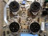
Below: Top side as received. Numerous parts never installed, various others removed. Circuit identifications on the board are mine.

Below: Bottom side as received. That is in fact 12 gauge stranded wire!!! Board notations are mine.

Below: Hey! Were'd yer phase inverter go???

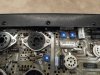
Below: Various unrelated parts were removed as well. The project apparently finally got reduced to parts board status....

Below: Lots of parts were installed, but lots never were all over the board.

Below: As noted, the bias supply. But instead of a .22 uF 100 volt transient suppression cap installed, that black lead is a direct short across the output of the rectifiers!

Below: Bottom side of the board: Even with the short removed, the bias supply still has problems! That transistor on the left has already been replaced once before, but there's no way the circuit will work because as shown as received, it's installed backwards! The transistor on the right has obvious problems, and even with all of this, the bias regulator is still non-functional because of missing components that were never installed........

Below: Beat up 3-T regulators. Both have broken leads -- primarily because the wrong heat sinks are installed. The heat sinks attached are woefully inadequate for devices dissipating nearly 2 watts each even if they aren't in the D115 operating environment. You may note that the board is drilled to mount the proper heat sinks, but if installed, they will short directly across the IN and GND terminals of both devices! Woops......... Note in all the board shots the lack of any board discoloration.
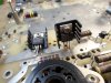
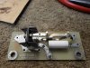
Below: Note how much bigger the proper sinks are, and the mounting feet they have to secure them to the board, protecting the device mounted to them.

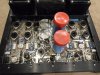
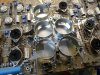
Below: A trial placement of the main electrolytic mount rings. Nearly two days worth of work was needed to carefully cut, trim, relieve, and orient the rings so that numerous parts on the board would not short to them, they would not interfere with the front chassis lip behind the transformers, and that the band tightening screws could still be accessed when installed. Incredibly tight clearances.......
More pics to follow.
Dave