@roger2 You're right about the course. I took another look at Udemy but this time closely examined a few courses on electronics, I purchased three. I am determined to learn.
@Goldie99 Interesting that you point out marking the schematic with references to faulty parts. You know, that dawned on my when I took a look at the schematic. The reason I used the PCB layout was to highlight which parts were found to be faulty (out of circuit). Thanks for the link on the transistor basics, I will check it out
I appreciate the input from the two of you.
@roger2 for the time being, I will be focusing on redoing a deck here at the house. I have to take advantage of the dry pause (we had rain lately). I will then be shuffling things around upstairs to make room for this NAD project. I will continue to check this thread in case but you might have something to instruct me on or ask. Once I settle some proper space upstairs for all things electronics I will be shifting most of my attention to learning.
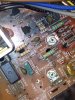
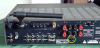
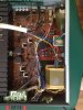
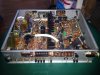
At the moment I feel confident that no real harm was done to the receiver, I have meticulous notes and photographic documentation on every step I took. I feel confident that nothing destructive took place but for two points.
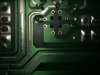
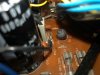
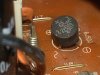
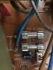
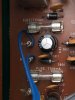
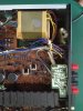
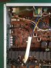
One traces was lifted but not torn (my bad for sure) - it's 100% intact but peeled slightly.
I did reflow and although my dwell time was short,
@roger2 pointed out that I may have caused some thermal stress to the more sensitive components layer on the PCB, possibly damaging them. Hopefully not.






 , no offense Alex...