• The move to the new server is done. There are some software and database maintenance updates in process. This has us passing the hat around to help out. We appreciate any donations. Seriously, even a dollar helps. The payment page may be found here - https://www.audiokarma.org/support.html

Sansui AU-717: Restoration with new boards

Is the AKL a plug in or how you get it in your library?

Yep, that is at least the easiest way to install it. Plugin and Content Manager -> Libraries -> Alternate Kicad Library. Then you'll find both the standard and the double libraries (for THT components only) in your footprint dialog.

Any reason you didn’t go for 4 layers PCB for dedicated ground planes ?

Importantly it's cheaper and I already have twice as many layers as Sansui used ;) A ground plane adds parasitic capacitance and I don't know in how far this would impact stability in this application. And since ground planes have a resistance as well, I wouldn't want to have "power" and "signal" return currents mix, so care has to be taken there too.
I think this isn't always quite as trivial as just adding a ground plane. But maybe it is in this case. If you (or someone else here) has experience with this, I'm always happy to learn... Would be a cool experiment for sure.
 
. If you (or someone else here) has experience with this,
I definitely do but unfortunately I have no numbers to present .
I made the AU-X11 PSU with 6 layers with dedicated layers for every CT ground .
The board is hosting rectifier/filtering/ protection circuit for the power amp VAS/EQ/Head amp (now flat amp for me ) and there is significant improvement under the 1000hz , with tighter and faster low end ,clearer SQ at mid low ( I’m running a 4way active) .
Again only my ears to trust , no numbers .
 
Wow, that's fancy! Did you publish any pictures etc.?

For the power supply board I would be less concerned with stability, more so for the driver boards. But I wouldn't be too surprised if it worked out just fine. For example the rather long NFB microstrip line has a length of ~10cm. Would guess 2-3pF/cm for a typical 4 layer FR-4 board => 25pF. Effective source impedance is ~1.17kOhm => pole at ~6 MHz. Probably still high enough that it doesn't matter. VAS stage? I don't know. I can add 10 or 20pF in my simple spice simulation model from various nodes to various other nodes and it didn't seem to matter too much stability wise. Maybe I did something wrong or it really doesn't matter that much...

But honestly, the cost were the main reason for not considering it seriously in the first place, regardless of whether this was clever :cool:
 
Believe me , if I don’t like what I hear after replacing “things” I just take them out and way to the garbage , regardless the cost or the “numbers” given to their datasheets.
The PSU made a huge deference to the audio quality, I’m not expecting to gain the same either from the pre-amp or the power amp, new boards .
Below is the board mounted …. I have a thread regarding the restoration of my AU-X11 from the beginning.
But lets do not pollute your excellent thread with irrelevant material , I was thinking starting a thread for Sansui re-designing PBCs/adaptors where we can share various projects .
 

Attachments

  • IMG_6467.jpeg
    IMG_6467.jpeg
    365.2 KB · Views: 26
I have a thread regarding the restoration of my AU-X11 from the beginning.
Thanks for sharing! I guess I have to look for this thread then ;) I'd love to get an AU-X1 (240V...) The only real reason I did not buy one a couple of weeks ago was the fact that I can't keep buying more and more amps. :D

I was thinking starting a thread for Sansui re-designing PBCs/adaptors where we can share various projects .
That's a great idea!
 
I'd love to get an AU-X1 (240V...)
I have the AU-X11 .

Mind that the X-1 and the X-11 are not only deferent in main voltage input .

I have uploaded the AU-X11 schematics in AK database where you can take a look your self.
Believe me it worth it !!!!
And actually if you do, with your knowledge and expertise we will much appreciate a comment on the topology !
 
Hello. Great idea to create a PCB thread/forum. We can share our projects. @SebastianH, how are you getting on with your PCBs? Are the Gerber files ready to be shared yet? I'm interested in them to rebuild a 717 I have stored away that's missing many parts. If you need any help and it's within my reach, let me know. Thanks.
 
Well, I noticed that I originally accidentally used 3.9k instead of 390 ohm resistors for R29, R30. Couldn't believe it. With 390 ohms (and without the clamp) the clipping performance is significantly worse, which is to be expected, actually. Fun. Maybe I'll try the KTA/KTC transistors with the 390 ohms.

I'm not happy with my rev C boards (this rev C is an experiment as well...). Still not a lot of room between the pre-driver heatsink for TR08 and the chassis. Works for the left channel board in my chassis, but since my right channel board is mounted slightly lower I figure there could be quite some tolerance from unit to unit. And there are other issues that I'm looking into (related to my experiment).

At some point it'll be ready to go, but unfortunately that's not the case yet ;) I'm sorry that you might be waiting for it, but I'm in no hurry - it's a hobby and shall remain that way...

I'll keep you posted about the progress :)
 
I tested clipping at 20 kHz with the clamps installed using 2x two BAT41 in series, left channel only (yellow trace). (R29/R30: 390 Ohm, CSC3503E/CSA1381E.)
Looks good to me. The waveform might even get (slightly) better with both channels clamped.

SDS2504X_Plus_PNG_21.png

I have changed the PCB layout once again (Rev D), hopefully the final revision of the driver board I'll build. (Btw.: I never ordered/built Rev B.) Major changes: No further experiments ;) Relocate some footprints for better chassis clearance.

The board can be populated differently:
  • Input low pass filter:
    • Positioned close to the JFET.
    • Positioned as in the original design.
  • Mounting options for dropper resistors R04, R10:
    • Bottom (recommend to keep some heat away from the electrolytic capacitors)
    • Front (not recommended! C04 will suffer!)
  • Optional MLCC footrprints for filtering of the Input pair power supplies
  • JFET:
    • LSK389A (tested). LSK389B might also work.
    • 2SK97 (untested, original design).
  • Long tail for the JFET input diff pair:
    • Two transistor constant current sink for the diff JFET pair; current settable with a trim potentiometer; or fixed by bridging the pot (tested).
    • Long tail resistor (untested, original).
  • Optional VAS stage clamps (tested).
  • VAS stage power supply filter with capacitor footprints allowing for D<=16mm, P=7.5mm and D<=12.5mm, P=5mm. Should allow for a ton of flexibility when choosing the capacitors, e. g. from 470uF/63V up to 820uF/63V for Panasonic FR series
  • Emitter resistor:
    • BPR58CR33J type resistor (metal plate, low inductance)
    • Wire-wound emitter resistors with a ceramic body (L<=22.4mm, W<=9.4mm, P=27.94mm) (similar to original)
  • Capacitor footprint (C21) in the Snubber network
    • P=10mm
    • P=5mm
  • Footprint for optional wires to reduce GND track impedance (like the on the original PCB)
  • Optional power indicator LEDs, SMD. Used in my testing for a quick visual feedback.
Rendering (with a couple of issues like the 3 pin connectors, don't care).

1777717933677.png

I hope to order Rev D tomorrow.
 
Great work on Rev-D @SebastianH

I am trying to understand the scope output above. How is this considered an acceptable waveform? When I scoped my AU 717 after restoration the 20KHz waveform was smooth with even clipping at 28V AC. I am sure I am not reading the waveform above correctly, please explain.
 
Thank you for asking critical questions, so I/we hopefully can learn something! A couple of things:

I actually do think the yellow waveform is acceptable (using the baker clamps mentioned in previous posts). Would you disagree?

Many amplifiers will have some additional distortion when clipping at 20 kHz. To be clear: The blue trace is the reason why I investigated further and implemented the baker clamp. And I'd love to try KSC3503/KSA1381, but do not have access to those, so I had to use CSC/CSA (KTC/KTA). I'd certainly prefer transistors that do not cause the distoration in the first place.

btw: I have not tested this, but my best guess is that the effect is caused by the transistors, not so much the PCB design itself. As always, I'm happy to be proven wrong.

a) Since restoration means different things to different people, what parts did you replace? And in particular, which transistors did you replace and by which type?
b) Do you happen to have scope screenshots/photos?
c) What was the slew rate before/after the restoration?
d) What was the THD before/after?
 
I did a FULL restoration on my AU 717. All transistors/capacitors were replaced with the exception of the drivers and finals. For VAS stage I used 2SC2911S/2SA1209S Sanyo transistors.

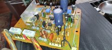
I have a basic scope on the bench (Rigol DS1054Z with firmware hack installed :cool:) Its pretty slow with FFT function with poor resolution so I did not measure THD. To test my work I do a freq sweep and also check waveform at 20Hz and 20KHz. I am trying to find a picture but I am positive the waveform was clean with even clipping with no kinks. Attaching a picture of the driver board from AU 719 to give you a perspective on the extent of restoration done (same was done on the AU 717 driver boards). You should be able to see the VAS transistors I used.

IMG_20240830_202057362_HDR.jpg

​

 
Very interesting! The Sanyo transistors are not readily available to me (shipping too expensive). I could get my hands on the CSC/CSA variants, might just order a couple of these and give those a try :) I could also test KSC2690/KSA1220, although those are not a perfect match for the VAS. Still, in my (simple) simulation the THD doesn't suffer too much.
 
Another option is to try TTA004B/TTC004B Toshiba transistors for VAS. These have a higher COB but still respectable. I have used these before (on AU 517 VAS stage) and they sound very good - but did not look at the waveform. These are readily available so you could try these.
 
Another option is to try TTA004B/TTC004B Toshiba transistors for VAS. These have a higher COB but still respectable. I have used these before (on AU 517 VAS stage) and they sound very good - but did not look at the waveform. These are readily available so you could try these.
I use the TTA/TTC in my AU-317 and I'm happy and with those (higher C_ob, yes, but this on is an EF-2, so at least the high gain ~200 should be somewhat beneficial). However, I tried the TTA/TTC and the measured performance was so much worse that I switched back to the CSC3503/CSA1381. Of course it could have been a measurement error as well. (I'm convinced that nobody could tell the difference in a properly done test either way.) Maybe I'll do one final test with a couple of transistors on the rev D board.
The clamp diodes don't have to be populated, but are there in case...

Btw: My amp will never be driven into clipping except during testing. If one encounters clipping, something has already gone wrong (for example wrong amp for the job). I'm more concerned with its performance in various normal operating conditions :D
 
I tested clipping at 20 kHz with the clamps installed using 2x two BAT41 in series, left channel only (yellow trace). (R29/R30: 390 Ohm, CSC3503E/CSA1381E.)
Looks good to me. The waveform might even get (slightly) better with both channels clamped.
I've never seen this tests and documentation here, thanks and great job.
 
I've never seen this tests and documentation here, thanks and great job.
Thank you - do you mean at 20 kHz specifically? I guess many people do clipping tests, maybe more often just at 1 kHz which is much more forgiving...

Just in case someone replicates it without thinking about it: I'd recommend to not go too much beyond 20 kHz at high output power levels or you might destroy something, for example the resistors (R46, R37; R46, R38) in the zobel network. This is true especially if clipping is present and/or you keep it there for longer periods of time:

Code:
Z_zobel = abs(R_zobel + j*X_C,zobel) = sqrt((R_zobel)^2 + 1/(2*pi*f*C)^2) = sqrt((10 ohm)^2 + 1/(2*pi*20 kHz*47nF)^2) ~ 170 ohm.

Sine wave without clipping at 85W into 8 ohm => U_rms ~ 26.1V:

Code:
P = R_zobel * I_rms^2 = R_zobel * (U_rms / Z_zobel)^2 = 10 ohm * (26.1 V / 170 ohm)^2 ~ 0.25W

=> no issue for the 2W original resistor (3W in my case)

But at 100 kHz the capacitor has a really low impedance: P ~ 5.4W (assuming the same amplitude as before).

Clipping waveforms have a lot of harmonic content and therefore the power dissipation can be significantly higher... And of course: frequency sweeps over the full bandwidth of an amp at maximum power may not be the greatest idea either :)
 
Last edited:
Back
Top Bottom