SebastianH
Member
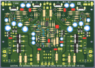
Quick update: Both driver boards (Rev D) are ready for testing...
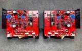
Initial results are fine.
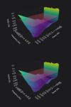
More results soon.
Initial results are fine.
More results soon.


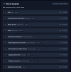

- A 10kHz square wave response into a capacitive load (8Ω∥2μF) to check phase margin and stability.
- IMD (Intermodulation Distortion) figures (SMPTE or CCIF).
- What kind of Slew Rate (V/μs) are these new driver boards achieving compared to the stock design?
Awesome work with the QA40x and test setup!
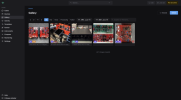
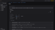
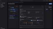
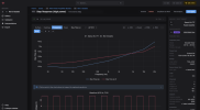
By the way, it’s fantastic news that you’ll be sharing the Gerber files in a couple of days! That is extremely generous of you and a huge contribution to the Sansui community. I’m definitely looking forward to downloading them and checking out your layout work.
Thanks again for sharing all these detailed test results!

1. On the Square Wave / Capacitive Load Test: Regarding 'what I had in mind': I wasn't looking for high-amplitude stress testing—1W (or ~8Vpp) into an 8$,\Omega$ dummy load with a 1µF or 2.2µF film cap in parallel is more than enough to evaluate stability.
)

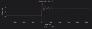
 But it's close enough to conclude that the amplifier works as expected, in my opinion.
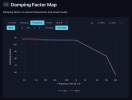
2. On IMD: Understood on the QA40x software/API limitations. Don't sweat calculating it manually from raw FFTs unless you really enjoy the coding part—the THD and Damping Factor maps you already provided paint a fantastic picture of the board's performance.
3. On Slew Rate: 32 to 36 V/µs is a stellar figure! That proves the new driver topology retains all the fast, wide-bandwidth character that made the AU-717 famous, while offering a modern, stable layout.
Regarding the F-2663 board: if you ever decide to share the Gerber files for that main PSU/Protector PCB alongside the Rev D driver boards, I’d be extremely interested. No pressure at all, of course—just wanted to compliment the layout work on it as well!

Thanks for the files. I am going to order these boards. Have a AU 717 for restoration. Will start with the driver boards. Once you release the power supply board will get that completed. Brilliant work and amazing contribution to our community of Sansui fansUpdate:
Gerber files of left and right channel driver boards published on my website. The website layout is a bit buggy, I'll fix it soon...
License is CC-BY-NC-SA-4.0. No commercial use. As is.
Link to the repo
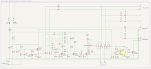
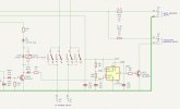
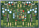

Will definitely report back, I am sure I will need some hand holding while populating the boards. Got six projects ahead of this as this so going to be around Nov before I will be working on this. Will keep this thread updated once the boards are ordered.You're obviously not obliged to report back, but I'd much appreciate feedback (and pictures). This would be especially important if something doesn't work as expected, so we can fix things before someone else orders the boards.
I would prefer to host the repository on a proper platform, but I'd also prefer not to use github. Maybe gitlab? I don't know
