• The move to the new server is done. There are some software and database maintenance updates in process. This has us passing the hat around to help out. We appreciate any donations. Seriously, even a dollar helps. The payment page may be found here - https://www.audiokarma.org/support.html

SX-580 120hz hum

they replace the 5 pin dual package ones . you have to tie 2 legs together .obviously the correct ones .

oh, I see. ok, so take two of these transistors and tie them together. Anything I need to measure or do before pulling them out? or am I good to just desolder and replace?

Does it matter which 2 legs? Just face them the same direction?
 
i tried looking but cant find now .
basically the emitters tie together . there should be markings on the board . data sheets are available for both transistor numbers .
 
i tried looking but cant find now .
basically the emitters tie together . there should be markings on the board . data sheets are available for both transistor numbers .
Got it
 

Attachments

  • Screenshot_20210804-174812.jpg
    Screenshot_20210804-174812.jpg
    44.9 KB · Views: 13
It does not. No testing on these I guess.
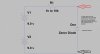
Build this little test jig, you can use it to test any pn junction, as well as STV diodes and zeners, just use 1 battery and an about 2.2kΩ to 10kΩ resistor, put the positive side on the anode or P junction side and the negative side onto the cathode or N junction side, and read the dc voltage on your meter:

ZenerTest3.jpg
 
  • Like
Reactions: J A
I'll build that today. So, I replaced put in the transistors. Left channel is now much much better at 12mVdc. The right channel, however something is wrong. I'm getting -23Vdc.

If there's a bright side to my awful skills at this. The left side one is so ugly and took so many attempts, that the path is torn up and I had to install a little jumper...that's the one that's working.

ugh, nevermind, I'm a hack at this point. fixing it now.

ok. left channel -64.7mVdc
right channel -112mVdc

These are final values I believe
 
Last edited:
Not quite sure where to go from here. DC offset numbers are improved substantially but obviously still not good.
 
Did you put in KSA992 transistors that had their base to emitter voltages matched? How did you measure that spec? Did you use that test jig?
 
I had already put them in when I saw your message, and it had been a dumpster fire so far (I'm having fun but making tons of really unecessary mistakes first before doing it right). Needless to say I'm down to the 2 pairs installed and 1 uninstalled pair.

Just a general question, will unpaired emitter voltages create that drastic of a DC offset without help from other components?
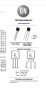
Footnote-I have 9V batteries on the way to the house now and I'll setup the tester.
 
Just a general question, will unpaired emitter voltages create that drastic of a DC offset without help from other components?
Yes, that is why the Vbe is matched, so the dc offset is minimized. The original 5-leg transistor was intended to be manufactured as a close spec pair, and the common package reduces thermal differences that can affect it. On some amps there is an adjustment, but not this one.
 
ah, I didn't understand the matched pair concept when I purchased. I thought "matched pair" meant just manufactured together/purchased together. I'm going to go back and order 2 matched pairs (exact terminology) this time.
 
You cannot usually buy matched pairs at a reasonable price (if at all). That is why I buy those kinds of transistor at the 100 quantity price, then match them myself (or yourself). Sometimes manufactured / purchased together is good enough, sometimes not. The 512-KSA992FBTA from Mouser is 14.1¢ each at quantity 100.
 
Last edited:
oh, I see. Well, I guess I'll buy 100 and measure/match them. Thanks for the clarification. I just misunderstood the whole thing I guess. I am shocked they make such a difference! Really interesting stuff.
 
The ac signal input to the differential amp is through C301 (C302) which blocks dc from the previous stage, and the is dc pulled/referenced at that base to ground [0vdc] by R301 (R302). There will be a very slight positive voltage at the base because the base current (very small) created a voltage drop across the resistor. The feedback from the output comes in on the other base, through R307 (R308) and the diff amp tries to keep the dc voltage there the same as the dc voltage at the input side. If there is a difference in the BE junctions that difference / error is 'magnified' at the output of the STK module. That is a very simplified description, but may help your understanding.
 
  • Like
Reactions: J A
Back
Top Bottom