• The move to the new server is done. There are some software and database maintenance updates in process. This has us passing the hat around to help out. We appreciate any donations. Seriously, even a dollar helps. The payment page may be found here - https://www.audiokarma.org/support.html

Working on a 2250B power supply, have a question

Just some advice for the future. DO NOT recap or change transistors on ALL of the boards at once unless you are experienced in doing so. Do one board at a time, then test. That way you know exactly what board you touched before it stopped working. If you do all at once it is very difficult to find the problem without going through all of the boards looking for an error in component value or polarity. :thumbsup:
 
Not J809 to J810! J809 to chassis ground. Then J810 to chassis ground.
Ahh, I see. Like I said I am a rookie. Here are those results I obtained this morning. These readings are with a cold reciever

J809-Chassis=000.4 This I can change with 707 pot

J810-Chassis=33.4 This I did not attempt to change.

so left channel is good, right is bad it appears?
 
Just some advice for the future. DO NOT recap or change transistors on ALL of the boards at once unless you are experienced in doing so. Do one board at a time, then test. That way you know exactly what board you touched before it stopped working. If you do all at once it is very difficult to find the problem without going through all of the boards looking for an error in component value or polarity. :thumbsup:
Ahh, this much I have been told/understand. I only recapped it and installed 3 transistors that came with my kit that were recommended for replacement (1318's) on the P800 board. I was hoping to find a bad cap or transistor on there that may have been preventing the relay from closing. Otherwise, I have not touched the other boards yet. But I am ready for more advice.

Thanks!
 
Thanks. It looks like (as you concluded) there is a problem with the P700 board since it has 33.4v on J810.
First... are your positive that you measured the voltage on J810 on the P800?
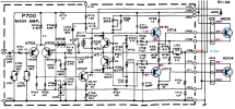
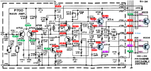
J810 connects to J709 on the P700 Main amp board as shown below.

1788276828453.png
Please do the following:
  1. Measure the voltage on J709 (it should match the voltage you previously measured on J810)
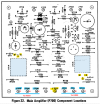
  2. Measure the ECB voltages on H003 and H004 (it may be easier to measure on the P700 board as shown below).
  3. Measure the ECB voltages on J714 and H715.
1788277431154.png
 
Thanks. It looks like (as you concluded) there is a problem with the P700 board since it has 33.4v on J810.
First... are your positive that you measured the voltage on J810 on the P800? Yes
J810 connects to J709 on the P700 Main amp board as shown below. OK

  • Measure the voltage on J709 (it should match the voltage you previously measured on J810) 33.4v confirmed
  • Measure the ECB voltages on H003 and H004 (it may be easier to measure on the P700 board as shown below).
705-41.2
706-34.08
708-33.48

711-41.3
711-33.48
712-41.3

H714
E-33.9
C-41.5
B-34.5

H715
E-33.9
C-41.5
B-34.5

  • Measure the ECB voltages on J714 and H715. I think you meant H714?
I was home on lunch and able to take time to read these. Hopefully I got it all. Be back in 3 hours TY!
 
Are all of the measured voltages negative? Some should be positive. You need to be careful to note the sign of the voltage because it makes a difference. You should typically use chassis ground as a reference for the black DMM probe. Something is shorted. Did you replace ANY of the transistors or capacitors on this board?

1788287661186.png
 
Are all of the measured voltages negative? Some should be positive. You need to be careful to note the sign of the voltage because it makes a difference. You should typically use chassis ground as a reference for the black DMM probe. Something is shorted. Did you replace ANY of the transistors or capacitors on this board?

View attachment 3828217
Hello, I am away from the reciever at the moment. I can redo the tests when I get in and note the +\- when I transcribe the results, which I was not thinking of at the time. I have not done anything to this board or the other board except remove and reinstall the output transistors for testing out of circuit.
 
Ok, I just re-measured everything. These were all taken with the common on my DVM clipped to chassis. I did not move it from there. The rest were taken with red probe.

I apologize for not providing polarity and using the dash in my numbering layout.

PINS as highlighted

705: +41.7
706: +34
708: +33.4

709, connected to P800 again as mentioned before +33.4

710: +33.4
711: +33.4
712: -41.5


715:
E: +33.25
C: -41.5
B: +33.25

714:
E: +33.9
C: +41.5
B: +34.5
 
Thanks for updating the voltages, unfortunately they are mostly all wrong.
There is one that is confusing: J711 = +33.4v which should be connected to H715 collector = -41.5v?
Please verify that the ground J713 is connected to chassis ground.
We need to isolate the source of the bad voltages.
Can you measure the ECB of H702, H703, H707, H710, H711 and J714?

1788303015361.png
 
Thanks for updating the voltages, unfortunately they are mostly all wrong.
There is one that is confusing: J711 = +33.4v which should be connected to H715 collector = -41.5v?
Please verify that the ground J713 is connected to chassis ground.
We need to isolate the source of the bad voltages.
Can you measure the ECB of H702, H703, H707, H710, H711 and J714?

View attachment 3828411
Thanks for updating the voltages, unfortunately they are mostly all wrong. Ok, that's not great, do you mean like they are not to spec, or I am giving you bad information that is not actually possible?

There is one that is confusing: J711 = +33.4v which should be connected to H715 collector = -41.5v?
I just double checked this??

Please verify that the ground J713 is connected to chassis ground. It is.
We need to isolate the source of the bad voltages. That would be great haha!
Just a note, I did not think that this had been worked on before me, but I am seeing some waer on the screw heads here where the board attaches to the standoffs.


Can you measure the ECB of H702, H703, H707, H710, H711 and J714? I will have to get these tomorrow
 
Just looking at the voltages you measured. It might be that H004 has a base to emitter short since they have the same voltage.
  • You can try removing H003 and H004 from the transistor sockets and see if it clears the voltage. Note which transistor went into each position so you don't mix them up.
  • Take a picture... just in case you need it.
  • Also, if you don't already have one, you should build a Dim Bulb Tester consisting of a switch, AC socket, and incandescent light bulb in a utility box with an AC cord. Look online to see how to build it. This will prevent a short from destroying other board components.
One more thing to verify is that H003 and H004 are connected to the correct terminals on the P700 board.
1788315502105.png
 
Last edited:
Just looking at the voltages you measured. It might be that H004 has a base to emitter short since they have the same voltage.
  • You can try removing H003 and H004 from the transistor sockets and see if it clears the voltage. Note which transistor went into each position so you don't mix them up.
  • Take a picture... just in case you need it.
  • Also, if you don't already have one, you should build a Dim Bulb Tester consisting of a switch, AC socket, and incandescent light bulb in a utility box with an AC cord. Look online to see how to build it. This will prevent a short from destroying other board components.
OK, well, I tested them out of the heatsink/connector and the consensus was that they were looking good.

I do have a dim bulb tester, and it was not running bright though at initial power up, so I went to full power. Hopefully that was not a big mistake. Should I be doing all of this testing under the dim Bulb Power?

I did get a bunch or all of these requested measurements just now

I was coming back to check on J714. we just need pin to chassis ground there? Otherwise, I will transcribe these tomorrow.

Thanks for sticking with me.
 
Thanks for updating the voltages, unfortunately they are mostly all wrong. Ok, that's not great, do you mean like they are not to spec, or I am giving you bad information that is not actually possible?

There is one that is confusing: J711 = +33.4v which should be connected to H715 collector = -41.5v?
I just double checked this??

Please verify that the ground J713 is connected to chassis ground. It is.
We need to isolate the source of the bad voltages. That would be great haha!
Just a note, I did not think that this had been worked on before me, but I am seeing some waer on the screw heads here where the board attaches to the standoffs.


Can you measure the ECB of H702, H703, H707, H710, H711 and J714? I will have to get these tomorrow

H702: E: +.56
C: -40.25
B: .12

H703: E: +.56
C: -40.8
B: +12.7

H707: I could not see ecb marking on this. but here are the values. I can take and upload a picture of the legs labeled if still needed but here are the values

: -41
: 33.5
: one was drifting while measuring. +.2 to +.3V

H710: E: +33.5
C: +34.3
B: +32.5

H711: E: +33.5
C: +41
B: + 33.1

J714: +35

If recommend I can pull the 003 and 004 tomorrow and carry on.
 
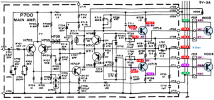
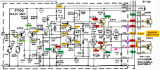
Added to the schematic.
Are you sure that H707 voltage of 33.5v was not -33.5v.
1788316533310.png
 
Last edited:
Added to the schematic.
Are you sure that H707 voltage of 33.5v was not -33.5v.
View attachment 3828557
Hello, I just double checked that 2875 at 707. it is indeed +33.5V.

I can do some more testing tonight if you have ideas.

Does there ever come a point where people just replace everything one by one on a board like this and start over to an extent? Obviously both would need to be done to match? Thx!
 
Generally speaking, you first find the source of the problem, repair it, then recap and replace any old parts as needed.

I think the next step would be to remove the two output transistors H003, H004 from the sockets (don't lose the mica insulator and note its location, not interchangeable).
You should be able to remove the two screws and pull the transistor out of the socket. Make sure the wires don't short when you power it back on.
Also, be VERY CAREFUL of that varistor clamped to the middle of the heatsink. Those are not available and the leads will just snap off.

Power on and re-measure the voltages on J705, J706, J708 and J710, J711 J712.
Next, re-measure the voltages on H714, H715, and H707.

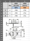
Here are the pinouts for H707. Please match up your voltages to the transistor pins and update if needed.
1788364067430.png
 
Last edited:
Generally speaking, you first find the source of the problem, repair it, then recap and replace any old parts as needed.

I think the next step would be to remove the two output transistors H003, H004 from the sockets (don't lose the mica insulator and note its location, not interchangeable).
You should be able to remove the two screws and pull the transistor out of the socket. Make sure the wires don't short when you power it back on.
Also, be VERY CAREFUL of that varistor clamped to the middle of the heatsink. Those are not available and the leads will just snap off.

Power on and re-measure the voltages on J705, J706, J708 and J710, J711 J712.
Next, re-measure the voltages on H714, H715, and H707.

Here are the pinouts for H707. Please match up your voltages to the transistor pins and update if needed.
View attachment 3828734

Good Evening. instructions followed. TY. I did all of this testing under 100W DBT. Hope that's OK.

ouput transistors removed and still tested good btw. I insulated the receptacles. They are still out of the machine. I rounded the numbers a bit

705 +38.5
706 +33.25
708 +29.25
710 +29.25
711 +29.25
712 -38.5

H 707 E: -37.5
C: +33
B: -37.8

H714 E: +33.25
C: +38.4
B: +33.8

H715 E: +29.3
C: -38.6
B: +33

I think I got it all, and double tested everything. Let me know if you think anything stands out. Thanks!
 
Put your latest voltages on the schematic with H003/H004 disconnected.
  1. According to the schematic H715 collector should be connected to J711 (H004 base) but you have two different voltages, one is + the other is -.
  2. Check the backside of the P700 board and follow the trace between these two points and see if there is a solder bridge or something connected on the backside of the board.
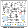
  3. If you can, take a good photo of the backside of the board (flat photo so I can match it up with the board layout in the SM).
  4. Does your service manual have a P700 layout that you can also see the board traces? My copy is poor and you can't see the traces.
1788400233239.png
 
Put your latest voltages on the schematic with H003/H004 disconnected.
  1. According to the schematic H715 collector should be connected to J711 (H004 base) but you have two different voltages, one is + the other is -.
  2. Check the backside of the P700 board and follow the trace between these two points and see if there is a solder bridge or something connected on the backside of the board.
  3. If you can, take a good photo of the backside of the board (flat photo so I can match it up with the board layout in the SM).
  4. Does your service manual have a P700 layout that you can also see the board traces? My copy is poor and you can't see the traces.
View attachment 3829052
Hmm, that is interesting. I could see that the pattern of voltages on the pins seemed odd, but double. checked and checked again. The receptacles for the outputs are definitely away from the underside of the board, but i left them in the heatsink to help keep it that way, and shimmed them against it with some foam. Here is a question so that I can remove the heatsink from the board to get the picture you want. What is the best way to remove the wires from the pins, as some are soldered, easy enough and some are the coils. I read that those coils can come off the pin and be reinstalled, but that seems unlikely to to me as that wire is brittle. Is there any truth to that? I know I have had one break in the past on a different Marantz due to handling while recapping and it was kind of odd to solder back to the pin. I feel like I am missing something on that process? thx and will figure it out tomorrow one way or the other.
 
What is the best way to remove the wires from the pins, as some are soldered, easy enough and some are the coils.
Don't remove the wires from the posts.
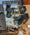
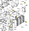
  1. You already removed the two transistors so the sockets should just come off of the heatsink.
  2. The only other component is the temperature diode (fragile), green arrow, that is held on to the heatsink with a screw (yellow arrow).
  3. You should then be able to remove the four corner screws that hold the board to the heatsink.
  4. You probably need to remove the bottom cover to get to the two screws.
  5. There should be two screws on either side of the heatsink that hold an L shaped bracket to the chassis or heatsink. Remove them to pull the board and heatsink if you can't get to the four board screws.
  6. The board should now separate from the heatsink.
  7. With the heatsink removed, you should be able to see the backside of the board.
1788406750883.png

1788405843951.png
 
Last edited:
Back
Top Bottom