• The move to the new server is done. There are some software and database maintenance updates in process. This has us passing the hat around to help out. We appreciate any donations. Seriously, even a dollar helps. The payment page may be found here - https://www.audiokarma.org/support.html

Working on a 2250B power supply, have a question

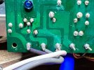
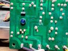
I read that those coils can come off the pin and be reinstalled, but that seems unlikely to to me as that wire is brittle. Is there any truth to that?
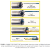
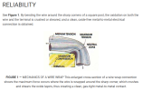
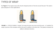
That technique of connection is called "wire wrap". The post is typically square and the wire solid. A tool is used to spin and wrap a bare wire around the post some 10 times. As you wrap the wire, it will "dig" into one of the edges of the post and form a solid electrical connection. It is very reliable because if you have 10 turns of the wire and four corners on the post, you will have 4 x 10 = 40 contact points to make an electrical connection.

You don't want to remove the wire wrap unless there is no alternative. Sometimes unsoldering the post from the board then resoldering is a better alternative.
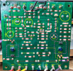
1788406255826.png
1788406308732.png
1788406338247.png
 
Don't remove the wires from the posts.
  1. You already removed the two transistors so the sockets should just come off of the heatsink.
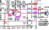
  2. The only other component is the temperature diode (fragile), green arrow, that is held on to the heatsink with a screw (yellow arrow).
  3. You should then be able to remove the four corner screws that hold the board to the heatsink.
  4. You probably need to remove the bottom cover to get to the two screws.
  5. There should be two screws on either side of the heatsink that hold an L shaped bracket to the chassis or heatsink. Remove them to pull the board and heatsink if you can't get to the four board screws.
  6. The board should now separate from the heatsink.
  7. With the heatsink removed, you should be able to see the backside of the board.
View attachment 3829110

View attachment 3829104
Wow, this is a great plan! and easy. I understand it from working on my 2240.
 
That technique of connection is called "wire wrap". The post is typically square and the wire solid. A tool is used to spin and wrap a bare wire around the post some 10 times. As you wrap the wire, it will "dig" into one of the edges of the post and form a solid electrical connection. It is very reliable because if you have 10 turns of the wire and four corners on the post, you will have 4 x 10 = 40 contact points to make an electrical connection.

You don't want to remove the wire wrap unless there is no alternative. Sometimes unsoldering the post from the board then resoldering is a better alternative.
View attachment 3829106
View attachment 3829107
View attachment 3829108
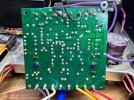
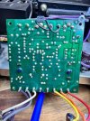
Wow, so simple, but effective! Maybe i read something about removing the pin itself. Ether way, great explanation. Here are those pictures which were easy to get this am.
 

Attachments

  • bottom of 7001.jpg
    bottom of 7001.jpg
    171.4 KB · Views: 9
  • bottom of 7002.jpg
    bottom of 7002.jpg
    179.6 KB · Views: 7
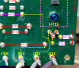
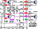
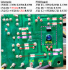
As far as I can tell, the schematic does not match the board. Image flipped to match SM board diagram.
  • H715 emitter on the board looks like it goes to R730 and J711
  • H715 collector on the board goes to R728
  • H715 base on the board goes to C713
But on the schematic, it shows:
  • H715 emitter goes to R730, but not J710
  • H715 collector goes to R728 and J711
  • H715 base goes to C713
Can you verify this or provide a clearer photo of that corner of the board so I can actually see the traces (need to adjust lighting).

1788452283725.png

1788452857345.png

Here is the board with components labeled. (image is flipped to match diagram in the SM)
1788453329596.png
 
Last edited:
As far as I can tell, the schematic does not match the board. Image flipped to match SM board diagram.
  • H715 emitter on the board looks like it goes to R730 and J711
  • H715 collector on the board goes to R728
  • H715 base on the board goes to C713
But on the schematic, it shows:
  • H715 emitter goes to R730, but not J710
  • H715 collector goes to R728 and J711
  • H715 base goes to C713
Can you verify this or provide a clearer photo of that corner of the board so I can actually see the traces (need to adjust lighting).

View attachment 3829328

View attachment 3829330

Here is the board with components labeled. (image is flipped to match diagram in the SM)
View attachment 3829339
I grabbed this at lunchtime. I think it will do. Your attention to detail is mind boggling. Thanks! Note: the board kinda looks like it took some heat there, or there was a manufacturing issue. That color change in the picture is not just lighting.
 

Attachments

  • 700corner.jpg
    700corner.jpg
    126.9 KB · Views: 6
  • 700v3.jpg
    700v3.jpg
    169 KB · Views: 7
Last edited:
OK, I compared your board to the schematic and they do not match. I wonder what else is not correct?

1788464969175.png1788465045255.png
 
OK, I compared your board to the schematic and they do not match. I wonder what else is not correct?

View attachment 3829445View attachment 3829446
Hmm, that's not good. I was given linked to this one redrawn by a AK member with my cap kit, which I mentioned earlier in this thread. There are some notes about different parts/values in the center bottom of it. Does this match the one you have been editing? Not a direct link as drive links to the index, but its there the 2250B Hires. It's a vector file, and I cannot screenshot it.

 
It looks like those corrections have been fixed in this version.

View attachment 3829578
Ok. So any idea what is going on at this point? I just dont know how to decipher all of this. i am more that happy to remove and test anything on that board. I am aslo curious, would it make any sense to disconnect this amp and prove that it will come out of protection and play music through the other channel?
 
would it make any sense to disconnect this amp and prove that it will come out of protection and play music through the other channel?
You can disconnect the bad board and see if the relay will click on the one channel. If it does, then the other board is good. If it doesn't then there may be another problem.
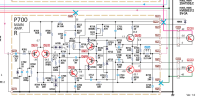
To do this you would need to disconnect the power leads going to the board from the Power Supply (blue Xs).
  1. Disconnect the 35v on J714
  2. Disconnect the 40V on J705
  3. Disconnect the -40v on J712
1788484851534.png
 
You can disconnect the bad board and see if the relay will click on the one channel. If it does, then the other board is good. If it doesn't then there may be another problem.
To do this you would need to disconnect the power leads going to the board from the Power Supply (blue Xs).
  1. Disconnect the 35v on J714
  2. Disconnect the 40V on J705
  3. Disconnect the -40v on J712
View attachment 3829674
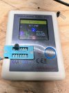
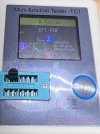
So, I am unsure where to go with this. But I was thinking, I fully remove the board by unsoldering the pins. Then I start testing each component. I have a set of the LCR meter tweezers, DMM, and transistor tester. If I get this off the receiver and start going through it one component at a time. I can also see if it comes out of protection as well. I have the 700 board new caps and a 702,703, 1nd 711 transistors slated for replacement, but I get the idea, fix it first then recap. I also probably have the other small transistors on that board in kit and could change them all so I know they are good. I have a lot of time this weekend and would like to make some progress. Any advice would be appreciated, including which parts need to come off to get correct reading and which do not. Thanks! -Marc
 
If it were me, I would not remove the board just yet.
Here is what we can try (all with power unplugged):
  1. First, I would like to update your measured voltages onto the corrected schematic
  2. Next, I would like to test the transistors that look suspicious using your transistor tester (you can try to test them in circuit, but it might not be accurate).
  3. You can try to test each of the electrolytic capacitors in circuit with your LCR meter. Depending on what other components are attached, your readings may be off and will need you to lift one side to test.
  4. We would replace any bad components, reassemble and power on to see if anything has changed.
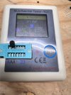
This might instruct you on testing a transistor with a DMM. Try it and see if anything looks suspicious. (I think when he says the meter reads 1, it is the same as OL or OC).
1788564566404.png
 
If it were me, I would not remove the board just yet.
Here is what we can try (all with power unplugged):
  1. First, I would like to update your measured voltages onto the corrected schematic
  2. Next, I would like to test the transistors that look suspicious using your transistor tester (you can try to test them in circuit, but it might not be accurate).
  3. You can try to test each of the electrolytic capacitors in circuit with your LCR meter. Depending on what other components are attached, your readings may be off and will need you to lift one side to test.
  4. We would replace any bad components, reassemble and power on to see if anything has changed.
This might instruct you on testing a transistor with a DMM. Try it and see if anything looks suspicious. (I think when he says the meter reads 1, it is the same as OL or OC).
View attachment 3830138
This sounds like a good plan to me. Do you just want me to test all of the transistors and caps?
 
Yes, try it without removing them and see what you get. Make a table of your results so we can review them.
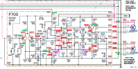
EDIT: Updated new schematic with your voltage measurements.

1788569447116.png
 
Last edited:
Ok, got it done. Not too sure how to best present the info, but here goes. All tests performed in circuit.

Caps: test good
701: 3.44/3.3
702: 10.4/10
704: 52.1/47
705: 43.3/47
706: 214.9/220

Diodes: just figured while I was there

H701: .615 WZ-177
H705: 1.012 1S2472
H708: .585 1S2472
H709: .589 1S2472
H712: .596 1S2472

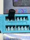
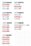
Transistors. I measured these in every possible direction. if it's not listed, it's OL. If this is not helpful in this way, I can retake them. first letter Black.

H702:2SA763, Manual, actual A7501 slated replacement 992
C>E=.816
B>C=.650
B>E=.660

H703:2SA733, Manual, actual A7501 slated replacement 992
C>E=.621
B>C=.603
B>E=.659

H707; 2SC875
C>B=.566
E>C=.562
B>E=.668
C>E=.644

H710:2SC945
E>C=.619
E>B=.072
B>E=.610
B>E =.072

H711:2SA733 slated replacement 992
C>E=OL
B>E=.079
B>C=.603

H714:2SD415
B>E=.610
C>B=OL
C>E=OL

H715:2SB549
B>E=rises1.5+++ cap?
C>E=.610
B>C=.604
.
Let me know what stands out. I can pull and test or whatever you recommend. Thanks!


Update: 9/5 AM. I took out 702,703, and 711. These are all to be replaced by 992's per my directions, so I figured I would take them out, and can either put in 992's or put these back. The parts list calls for 2SA763's in 702-703, but these were actually A7501's? quite a discrepancy in the 7501's
 

Attachments

  • H702-3(1).jpg
    H702-3(1).jpg
    129 KB · Views: 6
  • H711 2SA733.jpg
    H711 2SA733.jpg
    156.5 KB · Views: 8
  • H702-3(A750 for ID).jpg
    H702-3(A750 for ID).jpg
    131.1 KB · Views: 9
  • H702-3(2).jpg
    H702-3(2).jpg
    132.9 KB · Views: 8
Last edited:
Thanks for the transistor testing:
  • For your in-circuit testing, I have highlighted the suspect readings.
  • The CE junction should measure OC in both directions.
    • H714 looks suspect because the C to B is Open
    • H711 looks suspect because the B to E is almost a short
    • H710 looks suspect because the E to B is almost a short and the same as B to E
  • For the parts that you pulled (H702, H703, H711) could you use the DMM diode test both ways on the C-E?
1788622290372.png
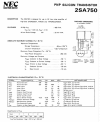
I looked up the two datasheets for the 2SA763 and 2SA750 (apparently = A7501)

1788622316329.png1788622341090.png
 
Thanks for the transistor testing:
  • For your in-circuit testing, I have highlighted the suspect readings.
  • The CE junction should measure OC in both directions.
    • H714 looks suspect because the C to B is Open
    • H711 looks suspect because the B to E is almost a short
    • H710 looks suspect because the E to B is almost a short and the same as B to E
  • For the parts that you pulled (H702, H703, H711) could you use the DMM diode test both ways on the C-E?
View attachment 3830601
I looked up the two datasheets for the 2SA763 and 2SA750 (apparently = A7501)

View attachment 3830604View attachment 3830605
First 750 test Cp.1(black)>Ep.2(red)=O.L Also open when reversed
Second 750 test Cp.1(black)>Ep.2(red)=O.L Also open when reversed
A733 test Cp.1(black)>Ep.2(red)=O.L Also open when reversed
All tested on DMM diode mode

Do I need to pull the other suspects?
 
I assume your notation Cp.1 is "collector pin 1" and Ep.2 is "emitter pin 2"?
Please also list the schematic reference no. (i.e. H714, etc).

H702: PNP, 2SA750 pin 1=E, 2=C, 3=B
First 750 test Cp.1(black)>Ep.2(red)=O.L Also open when reversed - E to C open both directions... no short​
H703: PNP, 2SA750 pin 1=E, 2=C, 3=B
Second 750 test Cp.1(black)>Ep.2(red)=O.L Also open when reversed - E to C open both directions... no short​
H711: PNP, 2SA733 pin 1=E, 2=C, 3=B
A733 test Cp.1(black)>Ep.2(red)=O.L Also open when reversed - E to C open both directions... no short​

Please check the following transistors out of circuit for E to C:
H707:​
H710:​
H711:​
H714:​
H715:​
 
OK, my mistake on that. The 702 and 703, I removed at the same time, same transistor type, but I forgot which one came from which spot.

H707 Marked D438E-5J C>E OL
H710: Marked C945A0962 E>C OL
H714 Marked 069 D415 E>C OL
H715 Marked 068 B549 E>C OL

keep me posted, Thx!
 
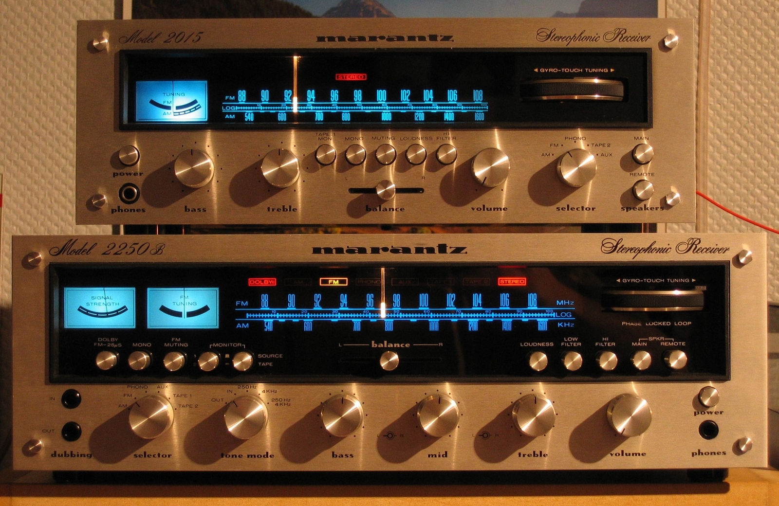
A wealth of worthy informations about the 2250B - thank you Guys !

Fortunately, my 2250B still works fine - like my other Marantz of the same era - and are still OEM...

mVKhJb-marantzBG2250B2015.jpg


a4ofOb-P1150468.jpg


T
 
Back
Top Bottom