

You are using an out of date browser. It may not display this or other websites correctly.
You should upgrade or use an alternative browser.
You should upgrade or use an alternative browser.
Yamaha A-1 JDM ( Silver face ) restoration .
- Thread starter Nashou66
- Start date
-
- Tags
- a-1 jdm a-1 yamaha integrated

Ahhh I was looking at the parts list which has a typo I would assume

I have some of these in 100 and 200 versions
https://www.vishay.com/docs/88736/sbyv27.pdf
Great thread, enjoyed going through it and looking forward to more ...
Thanks , I enjoy doing these types of threads as well.
Athanasios
Last edited:
The rest of my PS parts are not in yet. So I started to look at the Electrolytic Board.
Changed the two BP caps with Nichicon MUSE BP, installed the new relay. This was all done with the board in the chassis.
I bit heavy to move around on the bench but not a big issue.
The four heat sink transistors came out and were tested and inspected for proper thermal connection to the heat sinks.
Once again they where either bare or hardly any.

Also one was repaired by someone , maybe the same person who hacked the face plate and chassis.
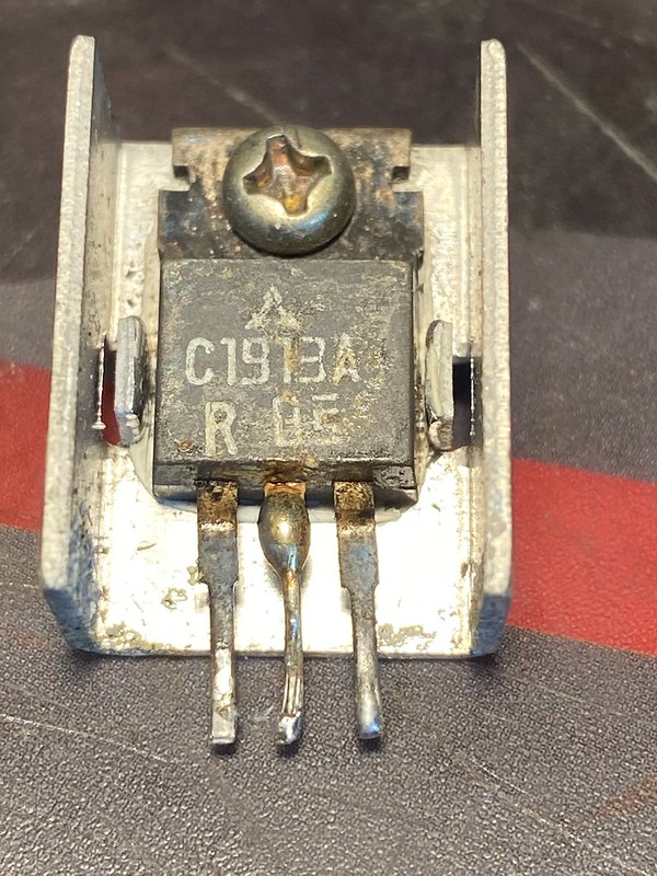
I had a couple in stock surprisingly , so I changed it out with the newer version that is all plastic case. hFE measured very close to the original so it worked out great.

Now onto the bias transistors that get pressed onto the heat sink. Now these should be
2SC1213 , as one was , it was an out house case style. The other was a 2SC2320 . Not sure why they went with that, maybe its all they had .

But its hFE is way different from the 1213's .

And the original 1213

And the new versions I have

As you see in the above pictures the pinouts are different, original are BCE and replacements are ECB .
So to get the flat side of the new version to be pressed against the heat sink I had to put some tubing over the E and B legs and twist them. Before I solder them in I'll ask you all if this looks right?

Athanasios
Changed the two BP caps with Nichicon MUSE BP, installed the new relay. This was all done with the board in the chassis.
I bit heavy to move around on the bench but not a big issue.
The four heat sink transistors came out and were tested and inspected for proper thermal connection to the heat sinks.
Once again they where either bare or hardly any.
Also one was repaired by someone , maybe the same person who hacked the face plate and chassis.
I had a couple in stock surprisingly , so I changed it out with the newer version that is all plastic case. hFE measured very close to the original so it worked out great.
Now onto the bias transistors that get pressed onto the heat sink. Now these should be
2SC1213 , as one was , it was an out house case style. The other was a 2SC2320 . Not sure why they went with that, maybe its all they had .
But its hFE is way different from the 1213's .
And the original 1213
And the new versions I have
As you see in the above pictures the pinouts are different, original are BCE and replacements are ECB .
So to get the flat side of the new version to be pressed against the heat sink I had to put some tubing over the E and B legs and twist them. Before I solder them in I'll ask you all if this looks right?
Athanasios
Parts came in today , Caps and Trim pots .
I installed the caps to the power supply board and the trimpot .

Uh oh!!!!! Wheres the trimpot?!?!?!?
Well I ordered the wrong type . For all the trimpots basically!!! Ugh
Oh well I guess I'll have to make them work as I hate wasting money and time. But I seem to do it often
So I moved it to the back of the board where the one resistor just above where the trimpot is would have gotten in the way for the type of Trimmer I got. I had to get creative with the legs and soldering them in.

I added hot glue to help hold down the trimmer for when it needs to be adjusted and any force wont
inadvertently break the solder joints.
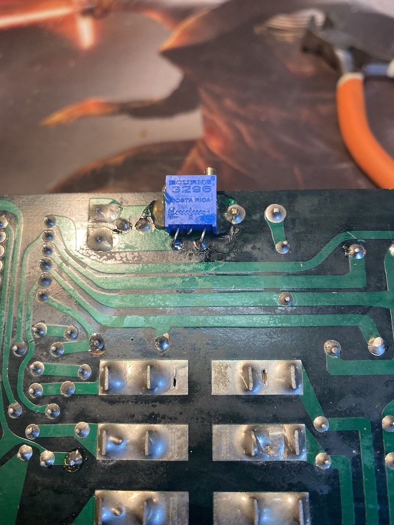
It does rise up above the edge of the board but I checked for clearance with the top on and it just barely is below the top.

I installed the 3.3uf BP muse caps to the tone board . The originals had extremely bad ESR
numbers, one was 12 ohms and the other was 23 ohms!!!! The new ones measured at 2.4 ohms each.
Much better for sure.
Also dont forget to re instal the EMI shield back to the bottom of the board.

On the volume board I again forgot that the trimpots are adjusted through a hole on the bottom of the PCB. I realized this as I went to remove the originals . And once again I had the wrong type. But I think these will clear the chassis and again I had to instal these on the bottom of the board.
These stand up on end and the proper ones should have laid flat. But then again there is no solder
pad on the top side. So maybe how I did it is the correct way. Unless you use trimpots that can be adjust from top an bottom as the originals. I just like the multi turn Bourns .

On the pre amp board I had the right ones!!!!

Remember to measure the original trimpots value and adjust the new one to that value.
Athanasios
I installed the caps to the power supply board and the trimpot .
Uh oh!!!!! Wheres the trimpot?!?!?!?
Well I ordered the wrong type . For all the trimpots basically!!! Ugh
Oh well I guess I'll have to make them work as I hate wasting money and time. But I seem to do it often
So I moved it to the back of the board where the one resistor just above where the trimpot is would have gotten in the way for the type of Trimmer I got. I had to get creative with the legs and soldering them in.
I added hot glue to help hold down the trimmer for when it needs to be adjusted and any force wont
inadvertently break the solder joints.
It does rise up above the edge of the board but I checked for clearance with the top on and it just barely is below the top.
I installed the 3.3uf BP muse caps to the tone board . The originals had extremely bad ESR
numbers, one was 12 ohms and the other was 23 ohms!!!! The new ones measured at 2.4 ohms each.
Much better for sure.
Also dont forget to re instal the EMI shield back to the bottom of the board.
On the volume board I again forgot that the trimpots are adjusted through a hole on the bottom of the PCB. I realized this as I went to remove the originals . And once again I had the wrong type. But I think these will clear the chassis and again I had to instal these on the bottom of the board.
These stand up on end and the proper ones should have laid flat. But then again there is no solder
pad on the top side. So maybe how I did it is the correct way. Unless you use trimpots that can be adjust from top an bottom as the originals. I just like the multi turn Bourns .
On the pre amp board I had the right ones!!!!
Remember to measure the original trimpots value and adjust the new one to that value.
Athanasios
Ok , next is re installing the heat sink/transistor assembly .
Here is one going in.

Dont forget to add some thermal past to the bias transistors before you put the heat sinks in.

The output transistor wiring re-soldered to the 'Lytic board.

Next is the re assembly of all the boards.
Athanasios
Here is one going in.
Dont forget to add some thermal past to the bias transistors before you put the heat sinks in.
The output transistor wiring re-soldered to the 'Lytic board.
Next is the re assembly of all the boards.
Athanasios
This part takes the most thinking of the whole restoration.
No matter how many pics you take you can still get easily confused. Next time I'll
take some notes of what I took apart first along with the wires that were desoldered.
But it wasn't too bad. A few harnesses looked similar but figuring it was helped by using the
silk screen labeling on the corresponding boards.
The first board from behind the faceplate to install is the last board I took out, which I forgot and why i need to take notes next time And that was the pre amp board.

There are three plugs to reinstall from the volume board( mentioned below again) and also the RCA connections, the three colored encased 4 wire harness's , Blue, red and Grey. These come from the back panel .
There is the GND harness's with the 3 black wires, and a harness from the 'Lytic board.
Also there is +/- 35 volt wire harness and another harness with a red and white wire that
also is a +/- 35 volt line. one comes from the 'lytic board and the other goes to another board. I believe the
Tone board IIRC.
The volume board is next and has three plug in harness's that get connected to the Pre amp board, #1,#2 and #3 Also make sure you feed the #4 harness between the pre amp board and the chassis so it can get plugged into the volume board. And there are the orange and blue RCA's that connect here. These are the MC signals as the head amp is on this board.
Here is the location fro the #4 harness fed between the pre board and chassis

Last is the tone board. This has a harness that fell apart and in the above pic as you can see. These get soldered to the tone board . Also there are two colored wire harness's that get soldered to the bottom of the Pre amp board towards the bottom. One under the plug in harness , this gets the white wrapped wires
and one between the bottom two switches , this is the red wrapped wires .
Here is the amp with all boards put back in.

And another, face plat on but knobs still not installed. Also need to address the lights. I thought I had one that worked but now none do. I may need to check the voltage for those.

All adjustments were made after a 20 minute warm up and dialed in nicely.
Tomorrow i'll hook up some speakers and check how it sounds.
there are some other small issues i'll talk about later.
Athanasios
No matter how many pics you take you can still get easily confused. Next time I'll
take some notes of what I took apart first along with the wires that were desoldered.
But it wasn't too bad. A few harnesses looked similar but figuring it was helped by using the
silk screen labeling on the corresponding boards.
The first board from behind the faceplate to install is the last board I took out, which I forgot and why i need to take notes next time
And that was the pre amp board.
There are three plugs to reinstall from the volume board( mentioned below again) and also the RCA connections, the three colored encased 4 wire harness's , Blue, red and Grey. These come from the back panel .
There is the GND harness's with the 3 black wires, and a harness from the 'Lytic board.
Also there is +/- 35 volt wire harness and another harness with a red and white wire that
also is a +/- 35 volt line. one comes from the 'lytic board and the other goes to another board. I believe the
Tone board IIRC.
The volume board is next and has three plug in harness's that get connected to the Pre amp board, #1,#2 and #3 Also make sure you feed the #4 harness between the pre amp board and the chassis so it can get plugged into the volume board. And there are the orange and blue RCA's that connect here. These are the MC signals as the head amp is on this board.
Here is the location fro the #4 harness fed between the pre board and chassis
Last is the tone board. This has a harness that fell apart and in the above pic as you can see. These get soldered to the tone board . Also there are two colored wire harness's that get soldered to the bottom of the Pre amp board towards the bottom. One under the plug in harness , this gets the white wrapped wires
and one between the bottom two switches , this is the red wrapped wires .
Here is the amp with all boards put back in.
And another, face plat on but knobs still not installed. Also need to address the lights. I thought I had one that worked but now none do. I may need to check the voltage for those.
All adjustments were made after a 20 minute warm up and dialed in nicely.
Tomorrow i'll hook up some speakers and check how it sounds.
there are some other small issues i'll talk about later.
Athanasios
Last edited:

Remodeling your bathroom ?tiled in nicely.

Remodeling your bathroom ?
lol Dialed in
Smart ass
But we have trouble.
I forgot to adjust VR 401 and 402 on the pre amp board. So I pulled the bottom off and
hooked up the dummy load set volume to 0 and began measuring to try to get to under 200mv per the SM instructions.
VR 402 test pint was 12 vdc !!!! Dialed that down but it fluctuates constantly under 200mv but goes from + to - in that range. So I left it.
but VR 401 at its test points measured 34 VDC !!!! WTF !! But this will not adjust.
But I noticed for a short time as i tried to adjust and putting pressure on the board it adjusted a little then the value went back up. Pressing on the 1 uf Yamaha film cap I was able to repeat it but only temporarily.
The fusible resistors all read ok
So I decided to also re check the other voltage adjustments.
The idle current was adjustable on the right channel but nothing on the left. all emitter resistors read ok.
and I now noticed the speaker relay does not click .
Both issues are on the left channel.
Should we start on the idle current adjustment or the pre amp eg DC offset adjustment.
And one thing I noticed Pressing the MM/MC button to MC lowers the voltage at VR 401 test points to about 4 VDC IIRC, did not write it down exactly what I pressed to get that, might have been the Disc button. Need to take notes next time.

Am looking over the schematic now but am stepping out in a while so I wont get to this till later.
Any help here would be awesome, so close to getting this done!!!
not looking forward to getting the Pre amp board accessible for any desoldering , ugh but its the only way
to get to it, the volume board needs to be moved.
Athanasios
Last edited:
I did a bunch of measurements on the TR's I could reach the legs with on the pre amp board , I always re check after I checked once, they kept on changing . Decided to check the fusible resitors( 47ohm 70ma ) and one on the left channel measure in the kohms. So There is one issue.
But I decided to get the idle current issue fixed first and then move onto the Pre amp issue.
the left channel is stuck at 3.4 mv idle current and can not be adjusted . Right channel is fine.
I decided to check the voltages on the BCE of the original TR 137 and they had 52 vdc. SO I pulled it to check it. Put it on my Peak DC 75 and it said it was good. Hmm put it back in. Now remember this is the Japan model and does not have the other two transistors TR 139 and 140. So I checked the resistors
R101,103,105 and FR101 all read ok in circuit.
So i decided to pull the output trannys and check those on the Peak, showed they are healthy.
What should I look at next? @avionic or @mbz ?
I think fixing this first is the right way to go unless you think the pre board should be sorted out first?
Athanasios
But I decided to get the idle current issue fixed first and then move onto the Pre amp issue.
the left channel is stuck at 3.4 mv idle current and can not be adjusted . Right channel is fine.
I decided to check the voltages on the BCE of the original TR 137 and they had 52 vdc. SO I pulled it to check it. Put it on my Peak DC 75 and it said it was good. Hmm put it back in. Now remember this is the Japan model and does not have the other two transistors TR 139 and 140. So I checked the resistors
R101,103,105 and FR101 all read ok in circuit.
So i decided to pull the output trannys and check those on the Peak, showed they are healthy.
What should I look at next? @avionic or @mbz ?
I think fixing this first is the right way to go unless you think the pre board should be sorted out first?
Athanasios
Last edited:
the left channel is stuck at 3.4 mv idle current and can not be adjusted
Is this in the left channel.. Where did you get the C1213 on the right ?
Is this in the left channel.. Where did you get the C1213 on the right ?
No the 1213 on the right allows the adjustment of the idle current. Not sure where I got them .But they measure close spec wise to the original on the left in the picture I took above.
I might have the channels wrong.
When looking at the electrolytic board from the top of the amp, the trim pot on the right side does not allow
idle current adjustment. I thought this is the left channel as LO is the same side as the original 1213.
Nashou
I Need to check the schematic but since the amp ios mostly DC any preamp issues may flow through to the main. Yeah that C1213 looks suspect fake, give me a momentDecided to check the fusible resitors( 47ohm 70ma ) and one on the left channel measure in the kohms. So There is one issue.
But I decided to get the idle current issue fixed first and then move onto the Pre amp issue.
EDIT: Check for VDC on the LI pin on the drive pcb
Last edited:
Bias transistor and VR closest to the LO pin is for left channelWhen looking at the electrolytic board from the top of the amp, the trim pot on the right side does not allow
idle current adjustment. I thought this is the left channel as LO
EDIT: Bias transistor in pic above on right appears for right channel
I Need to check the schematic but since the amp ios mostly DC any preamp issues may flow through to the main. Yeah that C1213 looks suspect fake, give me a moment
EDIT: Check for VDC on the LI pin on the drive pcb
C1213 in the right channel works fine , the one that was there and I replaced was a C2320
Between .8 and 2 its dancing around.
Bias transistor and VR closest to the LO pin is for left channel
EDIT: Bias transistor in pic above on right appears for right channel
Correct
Note VDC at the power supply pins +/-35V and +/-50V. Also measure Vdc at the LO, +I,,,CC pins (on the left side) These are the wire wrap pins not solder blobs in the vicinty of +/-I...
Crap measured at solder blobs but looks like they go to pins .


Off to bed back to it about 5-6pm tomorrow
Athanasios
Last edited:
My A1 kicked my butt so I'm not a good person to listen to, so I will take
a back seat and hopefully learn something. Basic observation being voltage measurements
showing high Vdc at the LI pin and the drive and main boards flooded with +ve
voltage. Could be FR503 or a shorted transistor or (more likely?) the LI voltage is shutting
down dual fet IC701 and the negative side of the amp. I'd sort out that LI offset voltage/FR
first.
Was the drive circuit offset adjust (VR501) successful?
a back seat and hopefully learn something. Basic observation being voltage measurements
showing high Vdc at the LI pin and the drive and main boards flooded with +ve
voltage. Could be FR503 or a shorted transistor or (more likely?) the LI voltage is shutting
down dual fet IC701 and the negative side of the amp. I'd sort out that LI offset voltage/FR
first.
Was the drive circuit offset adjust (VR501) successful?
My A1 kicked my butt so I'm not a good person to listen to, so I will take
a back seat and hopefully learn something. Basic observation being voltage measurements
showing high Vdc at the LI pin and the drive and main boards flooded with +ve
voltage. Could be FR503 or a shorted transistor or (more likely?) the LI voltage is shutting
down dual fet IC701 and the negative side of the amp. I'd sort out that LI offset voltage/FR
first.
Was the drive circuit offset adjust (VR501) successful?
After i did the restoration I was able to adjust all voltages. Only the pre amp DC offset i forgot to do.
On those test point I had 12vdc and 32 vdc where it should have been 200mv dc. I was able to adjust the
one but the other did nothing. then that is when i noticed the relay clicked off and all the troubles began.
So I am lost as well.
Maybe @avionic can help here?
Nashou
My A1 kicked my butt so I'm not a good person to listen to, so I will take
a back seat and hopefully learn something. Basic observation being voltage measurements
showing high Vdc at the LI pin and the drive and main boards flooded with +ve
voltage. Could be FR503 or a shorted transistor or (more likely?) the LI voltage is shutting
down dual fet IC701 and the negative side of the amp. I'd sort out that LI offset voltage/FR
first.
Was the drive circuit offset adjust (VR501) successful?
It was before. I had all voltages adjusted properly. After trying to adjust VR 401 and 402 on the pre board is when I realized things went south everywhere else.
I'll start with FR503 and 504 . Seems these FR's should be replaced all overt he amp, as a FR in the pre went high resistance on me.
Athanasios