• Please note that Audiokarma will be offline briefly for updates early on Monday morning, September 28th.

Yamaha A-1 JDM ( Silver face ) restoration .

View attachment 3007867View attachment 3007873

On the Electrolytic board, which test points get the black probe and which get positive? I originally just adjusted from stock down a couple points to 7.4mv, but now am wondering if I had it reversed and have my idle voltage set negative. The service manual illustration looks like its saying TP3 & TP4 are (+) and the center points are (-)

Here's a pic I took prior to making any adjustments:
View attachment 3007877
Polarity of the dc offset is not important. Keeping the offset below +/-10mv is.

You are on the right path if you have less than + /-10% at the test points and speaker posts.
Remember to do all adjustments after the amp temperature has stabilized.
 
Polarity of the dc offset is not important. Keeping the offset below +/-10mv is.

You are on the right path if you have less than + /-10% at the test points and speaker posts.
Remember to do all adjustments after the amp temperature has stabilized.


DC Offset on the Driver board and speaker terminals is within that +/- margin of zero and looking good, but my question is about the Idle voltage ("Indring current") - that doesnt matter either?

Because being +/- from zero is one thing, but this calls for being within 2mv of 7.4mv, does that mean -9.4mv is still ideal despite being 16.8mv off the specified target?

Screenshot 2023-10-12 at 1.41.18 PM.png
 
DC Offset on the Driver board and speaker terminals is within that +/- margin of zero and looking good, but my question is about the Idle voltage ("Indring current") - that doesnt matter either?

Because being +/- from zero is one thing, but this calls for being within 2mv of 7.4mv, does that mean -9.4mv is still ideal despite being 16.8mv off the specified target?

View attachment 3007983
Generic response: bias voltage is typically measured across a resistor and the voltage drop across that resistor (series with drain, source, emitter, collector, depending on the type of circuit and type of transistor) is indicative of the idle current of that circuit.


I am not familiar with the circuit of the A-1, test points, etc., so other answers would require some research on my part. Hoping that @avionic or someone with knowledge of this Amp could chime in.
 
Last edited:
DC Offset on the Driver board and speaker terminals is within that +/- margin of zero and looking good, but my question is about the Idle voltage ("Indring current") - that doesnt matter either?

Because being +/- from zero is one thing, but this calls for being within 2mv of 7.4mv, does that mean -9.4mv is still ideal despite being 16.8mv off the specified target?

View attachment 3007983
Disregard polarity indication on your multimeter. Or swap the test leads around if the ( neg ) sign bugs you..


Test procedure was written for and analog multimeter. Where analog meter swing direction comes into play.. And polarity of meter leads was important for a positive meter deflection.
 
Looking at the schematic I would have thought TP1 &2 would have a higher voltage, so +ve probe and black probe to TP3 &4 but as per avionic, I don't bother checking probe orientation, desiregard the sign.
 
Disregard polarity indication on your multimeter. Or swap the test leads around if the ( neg ) sign bugs you..


Test procedure was written for and analog multimeter. Where analog meter swing direction comes into play.. And polarity of meter leads was important for a positive meter deflection.

gotcha man, thanks, concerns alleviated :banana:
 
I went ahead and removed the output transistors and their associated heat sinks.

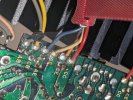
Here is the location of the transistor wires that connect it to the 'lytic board. Take a pic and desolder them all.

51826727236_3c66547469_h.jpg


Now that the transistor wires are desoldered from the 'Lytic board you can remove the 4 screws that hold the heatsink/transistor assembly from the chassis.

51826749216_596a9f778d_b.jpg

In regards to desoldering the transistor/heatsink sections, are both sides of the board soldered and re-soldered when putting it back? Didnt get a good look at your finished version

PXL_20231016_175043815.jpg
PXL_20231016_175112915.jpg
 
I put enough solder on the one side to make sure it flows through to the other side as well. But I always double check and then add more tot he side that needs it.

Athanasios
 
Back
Top Bottom