• The move to the new server is done. There are some software and database maintenance updates in process. This has us passing the hat around to help out. We appreciate any donations. Seriously, even a dollar helps. The payment page may be found here - https://www.audiokarma.org/support.html

2385 reconnect PS00 to P400 pin question

Thank you for clarifying that, it's just that you then stated on post #1015 that is a different order, testing the base to emitter first, NOT base to collector. If you didn't make this statement, I would understand but this is different than the order of your measurements.
And, yes you are not clear because you have two different measurement orders stated.
For now, I will assume that the table is correct and your description below is incorrect. OK?

"How testing was done and how to read results
On each transistor this was the order , Red lead on Base, black on Emitter. then Red on base, Black on collector .then Red on emitter Black on collector then i reverse
Black on base, Red on Emitter. then Black on base, Red on collector. then Black on emitter Red on collector."
Im just going to remeasure the listed transistors.
Red to base, Black to collector Red to base Black to emitter Red to collector Black to emitter then reverse
 
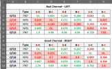
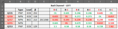
Just fill out a table that looks like this:

1788713729737.png

*** The other alternative is to pull out the 5 transistors in the bad channel (L) and test using a transistor tester, or 6 way test. That way there is no interference from the other parts of the circuit.
 
Last edited:
Just fill out a table that looks like this:

View attachment 3831430

*** The other alternative is to pull out the 5 transistors in the bad channel (L) and test using a transistor tester, or 6 way test. That way there is no interference from the other parts of the circuit.
Ok I will remove them tomorrow, I do have a transistor tester. I'm also thinking I should replace the resistors listed , that way there is no question of their condition
 
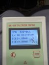
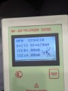
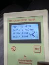
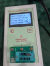
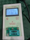
I tested the transistors and findings are as per photos, number on the photo is transistor number without the Q
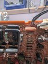
Also you can see a photo behind the board, the circled part was like that before the transistor was removed, not sure but i believe that needs to be jumped or that transistor can not work properly. That number is Q717
Even with the heat down to 320 c it is hard not to affect board, when i replace the transistors i will make sure all legs connect to trace.
Lastly if as i believe all of the transistors are good should i replace them with new ones. ?
 

Attachments

  • 717.jpg
    717.jpg
    66.4 KB · Views: 11
  • 719.jpg
    719.jpg
    62.6 KB · Views: 10
  • 721.jpg
    721.jpg
    82.2 KB · Views: 6
  • 713.jpg
    713.jpg
    73.8 KB · Views: 7
  • PXL_20260907_132425661.jpg
    PXL_20260907_132425661.jpg
    107.9 KB · Views: 14
Also you can see a photo behind the board, the circled part was like that before the transistor was removed, not sure but i believe that needs to be jumped or that transistor can not work properly. That number is Q717
OK, here is what I found.
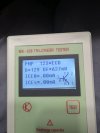
  • You tested Q717 and found an NPN transistor with leads 1=B, 2=C, 3=E with a gain of 118.
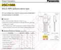
  • The PL shows this is a 2SC1568 (datasheet attached)
  • The pinout of the 2SC1568 is a NPN with leads 1=E, 2=C, 3=B, reverse of what you measured
  • What is the PN of what you pulled out of Q717 and why are the leads in reverse order?
  • Is it the same PN as Q718 for the other channel and mounted the same way?
  • Was the part mounted on the board backward or is it a bad part?
  • Let me know what you find.

1788793456554.png1788793590016.png
1788793882496.png
1788794962270.png
1788795309011.png
 
OK, here is what I found.
  • You tested Q717 and found an NPN transistor with leads 1=B, 2=C, 3=E with a gain of 118.
  • The PL shows this is a 2SC1568 (datasheet attached)
  • The pinout of the 2SC1568 is a NPN with leads 1=E, 2=C, 3=B, reverse of what you measured
  • What is the PN of what you pulled out of Q717 and why are the leads in reverse order?
  • Is it the same PN as Q718 for the other channel and mounted the same way?
  • Was the part mounted on the board backward or is it a bad part?
  • Let me know what you find.

View attachment 3831956View attachment 3831958
View attachment 3831960
View attachment 3831965
View attachment 3831968
Reading always from From left to right on how they are on the board Q713= ECB Q717 ECB Q721=BCE Q719=ECB
Photo of Q717 attached
When i test i always start from Base no matter which way it is installed , my readings reflect that
 

Attachments

  • PXL_20260907_154836663.jpg
    PXL_20260907_154836663.jpg
    125.5 KB · Views: 7
Reading always from From left to right on how they are on the board Q713= ECB Q717 ECB Q721=BCE Q719=ECB
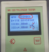
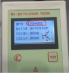
Yes, it matches the board, but when you tested the part in the transistor tester it reads 123=BCE, not ECB. Backward from the datasheet and your board layout.
There is something wrong with that transistor or your tester.
Your tester doesn't care which test lead is connected to which transistor lead. It determines that at tells you on the display. So in this case lead 1 = base, not emitter.


1788797962801.png
 
Last edited:
Yes, it matches the board, but when you tested the part in the transistor tester it reads 123=BCE, not ECB. Backward from the datasheet and your board layout.
There is something wrong with that transistor or your tester.


View attachment 3832004
If I put the transistor into the tester the other way it reverses the order . I will send a photo each way. It may just be the way I tested
 

Attachments

  • PXL_20260907_163833183.jpg
    PXL_20260907_163833183.jpg
    106.7 KB · Views: 13
  • PXL_20260907_163851213.jpg
    PXL_20260907_163851213.jpg
    110.4 KB · Views: 11
Transistors seem to be OK, but they don't match the other channel. You can put them back in and take voltage measurements of EBC voltages for all transistors and compare against the schematic. Maybe that will provide a clue.

When you tested the transistors before in post #1024, were they in circuit or out of circuit?
 
Last edited:
Transistors seem to be OK, but they don't match the other channel. You can put them back in and take voltage measurements of EBC voltages for all transistors and compare against the schematic. Maybe that will provide a clue.

When you tested the transistors before in post #1024, were they in circuit or out of circuit?
They were in circuit
 
Hi Dan im putting the original transistors back in today and jumping the trace with piece missing.
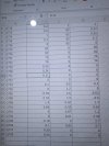
When i test for voltages, speakers removed and source and speaker off or connected,
 
Transistor voltages DC. some of the 0 are -
 

Attachments

  • PXL_20260917_222458961.jpg
    PXL_20260917_222458961.jpg
    126.8 KB · Views: 3
  • PXL_20260917_212526994.jpg
    PXL_20260917_212526994.jpg
    123.8 KB · Views: 3
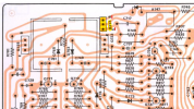
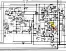
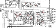
I don't know what happened to your board but almost all voltages are bad. (red=bad, green=OK, no color=not tested)
You are missing the -75V power coming into the board, also the -70V power???
You need to find out why.

1789690864886.png
1789690898531.png
 
Back
Top Bottom