• The move to the new server is done. There are some software and database maintenance updates in process. This has us passing the hat around to help out. We appreciate any donations. Seriously, even a dollar helps. The payment page may be found here - https://www.audiokarma.org/support.html

(another)Yamaha C-70 Project

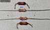
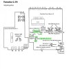
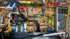
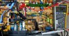
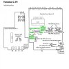
As the previous photos show, I removed R860, R859 and R863 to clean that area of the PCB. I could toss those components as the circuit they are part of will no longer be used.
Instead I will reinstall them, replacing R859 and R863 with new components...because they had glue residue. They won't be used but should some future owner want to restore the heater they will be there ready to use.

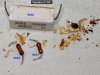
Here are the removed components and the residue I scraped off the board.
c-70_j01_pwr_on_switch_lamp_06.jpg c-70_j01_pwr_on_switch_lamp_07.jpg
 
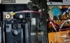
Here is the original C-70 power on lamp pulled from the switch housing.

c-70_j01_pwr_on_switch_lamp_08.jpg

Here is the LED replacement power on switch and its +15VDC power source.
I used a Visual Communications Company (VCC) VAOL-5701WY4 white LED, clear lens for the lamp. I added a 2.7KΩ load resistor.
On this C-70 project I added a yellow silicone lens cover to give the lamp a little more yellow hue as I thought it matched the original lamp better.

c-70_j01_pwr_on_switch_lamp_09.jpg c-70_j01_pwr_on_switch_lamp_10.jpg
 
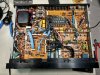
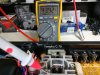
I moved the Yamaha C-70 over to a test bench today.
First thing was to check the power supplies.

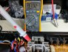
In other Yamaha C-70 post some folks asked about the power supply heat sinks being live with voltage when power is on.
The answer is yes...so always be very careful poking around and making measurements in the C-70 when power is on and the cover is off.
Here is what I mean...

c-70_j01_pwr_sply_on_01.jpg c-70_j01_pwr_sply_on_02.jpg c-70_j01_pwr_sply_on_03.jpg

When I make measurements in an amplifier I always remove power when placing the measurement probes on test points and component leads. It is too easy to have a slip up and short something out. In the above case with the C-70 there are some large metal areas with some thirty to forty volt DC so yeah, be careful.
 
The power supply voltages measure good in the C-70 so I moved on to the service manual General Adjustments page.
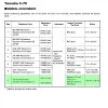
This page is not very clear to me. Plus there are some discrepancies between the service manual location of test points and the actual board.
For instance take Step 7, the Current Adjustment Equalizer circuit board.

yamaha_c70_sm_current_adj_eq_pcb_01a.jpg yamaha_c70_sm_current_adj_eq_pcb_01b.jpg

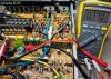
The actual location of test points 1 & 2 for the Left Channel I found here -

yamaha_c70_sm_current_adj_eq_pcb_01c.jpg

Test point 1 doesn't match up with Yamaha's C-70 service manual diagram.
The location of test points 3 & 4 for the the Right Channel matched up with the actual board and the service manual.
For both the Left & Right Channels I adjusted VR111 (Lch) and VR112 (Rch) to get 770mV ± 10mV across their respective test points.
I measured for DC voltage.

yamaha_c70_sm_current_adj_eq_pcb_01d.jpg
 
Last edited:
Next I went to Step 3 : 0dB AMP Adjustment Equalizer circuit board. Actually, I tried this first, got confused and jumped to the Current Adjustment Equalizer circuit board adjustments.
Now I am back to Step 3 which is a little confusing to me.
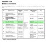
The service manual says this -

yamaha_c70_sm_0dB_amp_adj_eq_pcb_01a.jpg yamaha_c70_sm_0dB_amp_adj_eq_pcb_01b.jpg

If the measurement for the 0dB AMP Adjustment Equalizer circuit board is performed by measuring across resistors R335 (Lch) and R336 (Rch) for 0V ± 0.2mV then there is a problem with the right channel. I can adjust the left channel for 0 VDC but the best I can adjust the right channel is 13.9mV.

yamaha_c70_sm_0dB_amp_adj_eq_pcb_01c.jpg

That gives me a stopping point for today.
Am I measuring the 0dB AMP Adjustment Equalizer circuit board correctly for this service manual check.
If so then there is something off in the right channel.
 
Don't forget the Audio oscillator.
I think they meant to measure the steady state, power on, volume at zero, tone controls off...then measure the DC voltages of the output test points they list.
For the 0dB AMP Adjustment of the Equalizer circuit board I think it is across R335 and R336. So it appears the right channel has some issue. I will have to measure more points and compare the left and rights channels. Disappointing for sure as I was ready to test out how this preamplifier does on the audio analyzer.
 
Regarding Avionic's question about the black test lead on the 0dB AMP measurement...
It is on one side of R336 and the red DMM lead is on the other side.
 
Whew! Thanks for the save Avionic. I could have sworn I had tried that but obviously I didn't.
So Step 3 : 0dB AMP Adjustment Equalizer circuit board test is performed measuring from the R335/R337 node to ground (for the Left Channel) and from the R336/R338 node to ground for the Right Channel.

Doing that I get -
yamaha_c70_sm_0dB_amp_adj_eq_pcb_02.jpg yamaha_c70_sm_0dB_amp_adj_eq_pcb_03.jpg

So that step is a Pass. One possible worry there is that the Left Channel VR105 trimmer had to be fully turned counter-clockwise to get within the 0V ± 0.2mV spec.
It can't be adjusted any further.
 
It probably really doesn't matter which end of R335/336 you connect to.. It is a DC offset adjustment for the 0db amplifier.
 
Just for reference - Here are the diagrams for Step 3 and Step 7 adjustments showing the correct measurement points.

This one shows the correct location of TP1 for the Left Channel Current Adjustment (Step 7)

yamaha_c70_sm_current_adj_eq_pcb_02.jpg

This one shows that the Left and Right Channel 0dB AMP measurements are at the positions shown and made with reference to ground.

yamaha_c70_sm_0dB_amp_adj_eq_pcb_04.jpg
 
What about Step 1 (MC AMP Adjustment) and Step 2 (MM AMP Adjustment)? Are those just DC offset checks and adjustments?
Looks like it to me. Test points should read Left and Right REC out jacks.
 
Last edited:
What about Step 1 (MC AMP Adjustment) and Step 2 (MM AMP Adjustment)? Are those just DC offset checks and adjustments?
Look at what your actually adjusting. Your balancing the IC101 and IC102 +/- VCC to yield 0V dc offset at the outputs of the opamps.

IC101 and 102 are dual 4558 opamps.
 
Last edited:
Okay, I got the rest of the service manual General Adjustments made (for the DC offsets).
I am stuck on Step 6 now : Gain Adjustment Equalizer circuit board. It says to use a 150mV input so I take that to mean a 1KHz, 150mVrms sine wave into a source input (like Aux 1). Then measure the normal Pre-Out jacks for 1.5V ± 0.5dB. But at what volume level?
 
It says to use a 150mV input so I take that to mean a 1KHz, 150mVrms sine wave
Correct ( audio osc:thumbsup:) Volume control full CW.. Measurement made with (AC volt meter or O'scope :thumbsup:)
Balance control centered. Tone controls defeated/ by-passed.Filters -off..
 
Last edited:
Back
Top Bottom