

You are using an out of date browser. It may not display this or other websites correctly.
You should upgrade or use an alternative browser.
You should upgrade or use an alternative browser.
Brainstorming a push-pull 6L6GC stereo amp
- Thread starter thorpej
- Start date
-
- Tags
- 6l6gc push pull ultra linear

Please take a look at the voltage across the capacitors and the diodes with the sim. I'm not sure where to get 800uF capacitors with the proper voltage rating. I guess you will have to do some series and parallel combinations.
AES carries JJ 800uF 385V can caps. 385V should be just fine because it's the difference between the + and - terminals of the cap that you're concerned with. Hm, though I am a little confused looking closer at the simulation ... the cap in series with the bottom leg of the PT seems to have a higher voltage on the - terminal than the + terminal. I referenced a canned topology for that multiplier, so *boggle*.

Jaz--your comment made me go back and analyze this quadrupler more closely. I think there is a typo on the original schematic. While I do believe the 350V rating on each individual cap is sufficient, the lower cap appears to be connected in backwards polarity.
Thorpe--you may want to investigate this on your own simulation.
Thorpe--you may want to investigate this on your own simulation.
Jaz--your comment made me go back and analyze this quadrupler more closely. I think there is a typo on the original schematic. While I do believe the 350V rating on each individual cap is sufficient, the lower cap appears to be connected in backwards polarity.
Thorpe--you may want to investigate this on your own simulation.
Yah, I came to the same conclusion -- see my post above yours. As far as I can tell, there's never more than 220V across each cap, but yah, the lower cap seems flipped around. I can't figure out how to specify cap polarity in LTspice (on the assumption that if I could, the simulation would tell me "your cap just exploded!"). I think this may have been why I was having so much trouble following the charging path when you first pointed me at that circuit.
Anyway, these are the caps I planned to use: https://www.tubesandmore.com/products/C-EC800-385

The two caps connected to the transformer primary should be rated for at least the full peak voltage of the transformer. The two at the output of the quadrupler should have twice that rating.
Right, the Vpk of the transformer is 109 (78Vrms). 250V-rated caps would be sufficient, but I'm planning to use 385V-rated caps.
So, I have continued to fiddle around with this. I think I have the high voltage supply pretty much worked out:
- 4x voltage multiplier spitting out 415V. Ripple at the output of the multiplier is 4Vp-p.
- First tap on the power rail feeds 2 independent filters for the output stage supply -- each one a 2.5H 300mA choke + 100uF cap. It simulates at a pretty smooth (ripple .035Vp-p) 410V at idle (125mA per channel is what I ballparked).
- Second tap on the power rail is filtered by a 300 ohm resistor and a 500uF cap, feeding both of the differential pair inverters. I ballparked the current at 10mA per triode, so 40mA total. This simulates at right around 402V, BUT... this stage has the most ripple because it only has one filter. The simulator shows 0.04Vp-p. I suspect I'm getting worked up over nothing, but I wish it were smoother.
- Third tap on the power rail is filtered by a 56K resistor and a 10uF cap, feeding both triodes of the AF amp stage. This simulates at a pancake-flat 213V at a 3mA idle.
- Final tap on the power rail is a 470K + 75K voltage divider that serves as a bleeder and provides 30V of heater elevation.
Attachments
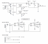
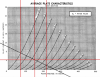
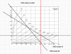
Spent some more time on this over the last week or so and I think I'm ready for sanity checking... Drew up the load lines and figured the current that would be present at each tap on the power rail, adjusted the supply accordingly. Attached are the load lines I drew up for the various stages, and a PDF that contains the schematic for my the ridiculous power supply and one channel of the amplifier itself (there will be two). Yes, it does look quite a bit like an Eico HF-89. I think I have the gain of each stage calculated correctly (wasn't 100% sure about the differential pair inverter, but it seems plausible).
One thing I'm still not 100% certain about is the bias supply. I'd really like to be using larger grid return resistors for the 6L6GCs, but I'm wanting to keep under the 100K limit when the total resistance of the bias supply resistor network is included. As I understand, this is a bit fungible if I have sufficient current the bias supply, but I'm having trouble getting LTSpice on the Mac to give me current through 0V voltage sources.
One thing I'm still not 100% certain about is the bias supply. I'd really like to be using larger grid return resistors for the 6L6GCs, but I'm wanting to keep under the 100K limit when the total resistance of the bias supply resistor network is included. As I understand, this is a bit fungible if I have sufficient current the bias supply, but I'm having trouble getting LTSpice on the Mac to give me current through 0V voltage sources.
Attachments

The gain of the cathode coupled differential pair seems low. I'm thinking it should be somewhere between 5x and 7x from each output to ground. That means with 12 dB feedback you probably don't need the cathode bypass on the 12AX7, or keep the cathode bypass but add a bit more feedback.
The gain of the cathode coupled differential pair seems low. I'm thinking it should be somewhere between 5x and 7x from each output to ground. That means with 12 dB feedback you probably don't need the cathode bypass on the 12AX7, or keep the cathode bypass but add a bit more feedback.
Yes, I should have mentioned that... that one is troubling me, too. Looking at the load line, the gain should be in he ballpark of 15. Using the standard gain calculations, it's more like 14, but that assumes fully-bypassed cathode. This jives with your estimation. 1.8 should be right for a non-bypassed cathode. I'm not sure how to handle this with a CCS. That said, I can't recall ever seeing a long tailed pair with a cathode bypass capacitor?
My preference would be to keep the -12dB but eliminate the cathode bypass cap on the 12AX7, which should keep that stage more linear and provide some additional headroom, and would still be a reasonable amount of gain (33 instead of 58).

jazbo8
Well-Known Member
An AC bypassed cathode will remove all the differential signal, thus defeating the stage's fuction.I can't recall ever seeing a long tailed pair with a cathode bypass capacitor.
A stage gain of 14 would be the differential gain. Gain of each output with respect to circuit ground would be 1/2 of that.
Ok, so does that mean for the purposes if calculating the overall open loop gain I use the the 1/2 figure? (Sorry if this is a dumb question...)
Yessir. Well I guess it depends on the method, but the method I use is based on the amplitude of the drive signal needed to push the output stage to full power. In your case (from memory) I think that's about 25V RMS if I recall where you have your output stage biased. So amp sensitivity open loop is about:
25/(7.5*33) = 100mv
(assuming 33x gain with unbypassed cathode on first stage)
and with 12 dB feedback (feedback factor of 4x), sensitivity would be 4x of that.
25/(7.5*33) = 100mv
(assuming 33x gain with unbypassed cathode on first stage)
and with 12 dB feedback (feedback factor of 4x), sensitivity would be 4x of that.
jazbo8
Well-Known Member
Which 0V voltage source? Where is it in the circuit?I'm having trouble getting LTSpice on the Mac to give me current through 0V voltage sources.
Yessir. Well I guess it depends on the method, but the method I use is based on the amplitude of the drive signal needed to push the output stage to full power. In your case (from memory) I think that's about 25V RMS if I recall where you have your output stage biased. So amp sensitivity open loop is about:
25/(7.5*33) = 100mv
(assuming 33x gain with unbypassed cathode on first stage)
and with 12 dB feedback (feedback factor of 4x), sensitivity would be 4x of that.
Right, ok... so, open loop gain is then 33 (non-bypassed 12AX7), 7 (differential inverter), 10 (output tubes), 0.07 (transformer) = 161.7
Then, closed loop gain with -12dB feedback: 8.25, 7, 10, 0.07 = 40.4
(For the purposes of calculating the feedback network)
And for input sensitivity... Yup, I use the same method to calculate that as you do (yah, tubes are biased at -35V right now, so 25Vrms is about right). Cool. Still < 500mVrms, so a very sensitive amp. I suppose that means I can get away with more feedback, but I'll make that decision after I actually build it, I think.
I am really liking how not bypassing the 12AX7 cathode worked out. This should make for a nice low-distortion front-end.