• Please note that Audiokarma will be offline briefly for updates early on Monday morning, September 28th.

Sansui AU-719 Protection Problem

bobpep

New Member
As Found Condition: The AU-719 is in protection when both the L channel or R channel Driver Boards are installed and there is a positive DC voltage on the output of both Driver Boards. With either Driver Board is installed by itself the protection issue persists. When both Driver Boards are out of service the amp comes out of protection and all of the amps DC bus voltages check normal.

TR12 is biased off by this condition and all of the voltages around the input dual N Channel JFET don't agree with the schematic. Checked all of the individual components on both Driver Boards in and out of the circuit and they all checked within specification.

Has anyone experienced this condition, and if so, can you please point in the right direction toward a solution?

Thank you,

Bob
 
Register to hide this ad
As Found Condition: The AU-719 is in protection when both the L channel or R channel Driver Boards are installed and there is a positive DC voltage on the output of both Driver Boards. With either Driver Board is installed by itself the protection issue persists. When both Driver Boards are out of service the amp comes out of protection and all of the amps DC bus voltages check normal.

This paragraph covers a lot of territory. It might be helpful for you to be pretty specific about the conditions you're seeing when in/out of protection, e.g. what is the voltage you measure on the driver board outputs, what do you mean by the driver boards being 'out of service' etc.

That said, there are lots of 719 protection and restoration threads here with lots of valuable info, search is your friend in this case :)
One topic that might be helpful is the discussions about symptoms of the failing SCR on the protection board, look for posts by @Hyperion on this one
 
"Driver boards out of service" likely means when the boards are removed from the amp. Basically he's saying that when both boards are installed or just 1, the amp goes into protection, but when both driver boards are removed it does not get stuck in protection. Most likely the problem is on the driver boards since when they are removed the amp comes out of protection but when 1 or both are installed the amp goes into protect mode.

It was stated that "all individual components were checked in & out of circuit and all were within spec." But based on the symptoms it seems like the problem is on the 1 or both of the boards. Would help other members here to explain what components you checked & how or what you checked on them. Also close up pics of the boards and the numbers you said were within specification. I cant help much on checking each component or what they should show but there are some known problematic parts in the 719 like black flag caps that can cause problems and should be changed ASAP as well as corrosive glue on the big caps that can cause problems.

On my 719 I recently repaired that had similar symptoms and a dead left channel, all smaller parts tested OK and when the left board was removed the amp came out of protect... the problem on the left driver board ended up being the main output transistors, they were replaced with no name at some point in the past, I replaced the outputs on both sides with recommended Sankens and the amp works & sounds great, did a full electrolytic recap and removed the bad sansui glue.

Post more details & some pics, Im sure the Sansui experts here can get your amp up & running again.
 
Bob, just to be clear, I think we're all happy to help out with your debug, how's it going?


Here's a couple of links to good discussions:


Thanks for all the helpful feedback, it’s greatly appreciated.

I’ve been referencing all of the forums pertaining to my AU-719 amp prior to posting this thread, and it has really helped me.

To answer some of your questions:
1. I did replace the protect circuit SCR with the P0102DA 1AA3 as suggested and the amp still doesn’t come out of protection.
2. The glue problem has been corrected.
3. Both Driver Boards have gotten the Lee Stereo Restoration/Upgrade treatment.
4. The Four main power supply electrolytic capacitors have been replaced with 10,000ufd 100v Nichicon capacitors.
5. All of the Driver boards transistor’s have been replaced with the recommended Sansui Forum’s transistor substitutions threads, except for the NEC u
 
It looks like my thread got truncated. I was having problems sending this thread prior to this truncated post being sent. Will try later with the remainder of the post. Thanks for your patience.

Bob
 
The amp is most likely in protect because of DC offset or bias being off.
Have you measured and adjusted these on both boards?
Since the relay won't switch you have to measure DC offset on the amp boards or the protect board.
 
Continuing :
5. ... except for the two NEC uPA68h N Channel JFET's.
6.The four trimmer's were replaced on the Diver boards, but not the ones on the Phono EQ board because they worked okay and the new trimmers were a pain in the neck to adjust.
7. All Black Flag capacitors were replaced.
8.Both Driver Boards were reflowed and any damaged pad were repaired. and the same for the rest of the amp.
 
What Magnus said above .
If you replaced trimmers and transistors then need to adjust DC offset and bias .

If the relay is not clicking you need to measure as close as possible to 0mv before the relays .
 
Currently, I'm marking the F2926 and F2927 schematics with the "as found" voltage readings for submission for your review and comments.

VR01 is set to the center position and VR02 is set to the fully CCW. I'm using the DBT, and with +/- 10 volts applied to the rails of F2926 I'm reading +8.6 volts on Terminal 13 (output) of the F2926 board. Basically, TR10,TR13, and TR15 are on and TR12, TR14, TR16,TR701 and TR703 are off. TR17 has Vb = +6.0 v, Ve = +5.5 v, Vc = +5.5v; TR11 has
Vb = +8.8 v, Ve = + 8.6 v, Vc = +9.8 v.

Is this a DC offset and bias issue or a problem with the Input Stage?

Note: When I'm trying to post to this thread I keep getting AK Oops messages and to try again later, could this be a problem with my VPN software?
 
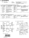
8.6V on pin 13 is way too high, it should be zero. See step 1 from the Service Manual below.
Have you tried adjusting with VR01 to see if it affects the offset?


1774276898473.png
 
That's what I was looking for when I measured it. By way, I have the AU-719 service manual. The best I could get was +6.6 v DC using the VR01 trimmer dialed to its limit.
Can you recommend trimmers? The Bourns trimmers installed are not multiturn and are not doing the job. I searched online and got the following recommendations:
3296W-1-101LF, 3296W-1-501LF or 3296Y-1-501LF. Do you use these types in your amp?

I had some initial success with the F2927 ( F2926 removed) driver board installed at lower (+/_ 10-15 v DC) DC rail voltages adjusting Offset and bias, but when raised to +/- 20 v DC the output voltage shot up to +8.6 v DC and I could only drop it to + 6.6 v DC as before.

But with either F2926 or F2927 driver board installed in the amp one at a time, when the Variac Voltage = 66 v AC and Kill A Watt Voltage = 51 v AC, the DBT bulb brightens and
gets much brighter as the Variac Voltage is increased but the Kill A Watt Voltage remains around 51 v AC.

Thanks for all your help, I really appreciate it.

Bob
 
It sounds to me like you have the bias turned all the way up - that's why the DBT bulb gets bright, and also why the AC voltage is low - because I am thinking it's being pulled down by the excess current draw.

The unit isn't coming out of protection mode because the DC offset is far too high, and you are unable to adjust it - as you have the problem with both OR either driver board installed you have a fault on both driver boards OR something wrong with the output transistors. DC offset is a balance adjustment, unless the positive and negative halves of a channel are working equally, meaning they are balanced, you'll never be able to adjust the DC offset.

You need to check your work, maybe a transistor (on both driver assemblies) installed incorrectly, or maybe an NPN/PNP confusion?

Sometimes, with some units and DBT bulb combinations people find that they can't get the unit out of protection mode with the DBT installed - whatever you do DO NOT remove the DBT for the time being - we need some clarity about whether the bias can be, or has been, adjusted.
 
Last edited:
Completed the F2926 Driver Board checks and the only odd readings I found were the following:

T10 PNP In Circuit: Vbe = 0.500 v, Vbc = 0.558 v; Out of Circuit: Vbe= 0.625 v, Vbc = 0.621 v, Vce = OL
TR12 NPN In Circuit: Vbe =0.500 v, Vbc = 0.558 v; Out of Circuit: Vbe = 0.629 v, Vbc = 0.629 v, Vce = OL

TR 11 NPN In Circuit (VR02 fully CCW): Vbe = 0.518 v, Vbc = 0.615 v; In Circuit (VR02 fully CW): Vbe = 0.593 v, Vbc = 0.615 v.

In Circuit: R34 (47 K ohm) = 24.61 K ohm; Out of Circuit R34 = 46.93 K ohm
In Circuit: R35 (47 K ohm) = 24.85 K ohm ; Out of Circuit R35 = 46.72 K ohm

Could find no incorrectly installed components.
All resistors were found in circuit to be within there 5% tolerances except for R34 and R35.
All transistors, diodes, JFET's, zener diodes tested okay in circuit except for TR 10 and TR 12 and possibly D01 and D02 (see below).
All electrolytic and 1 ufd film capacitors tested okay in circuit.

I found D01 = 1.306 v and D02 = 1.316 v in circuit, I thought they would read closer to 2.0 v, are these readings okay?

Bob
 
Is this when you power up on a DBT only? I.e. no lower voltages from a variac or similar?
Is VR1 set to middle and VR02 set to full CCW?
 
Is this when you power up on a DBT only? I.e. no lower voltages from a variac or similar?
Or, are you reporting measurements with an unpowered 2926 board?

I'm not sure if you said you had tested the output transistors, if not, now is a good time to do that.

All resistors were found in circuit to be within there 5% tolerances except for R34 and R35.
All transistors, diodes, JFET's, zener diodes tested okay in circuit except for TR 10 and TR 12 and possibly D01 and D02 (see below).

I found D01 = 1.306 v and D02 = 1.316 v in circuit, I thought they would read closer to 2.0 v, are these readings okay?

Keep in mind, measuring R34 or R35 (or ANY resistor) in circuit will measure the resistor in question in parallel with ALL the other current paths between the pins of the resistor. In this case R34 is in parallel with the series combo of R30, R32, VR02 and R35, so about half the of 47K is OK. Trust the out of circuit measurement.

Likewise with TR10 and 12, I'd trust the out of circuit test, your meter or tester may limit the current available to turn on the BE and BC junctions and that will make the voltage appear lower than you'd expect.

D01 and D02 are in a similar situation, there is a parallel current path with 2 junctions for both when in circuit so your tester is not measuring what you want. You would need to pull them out of circuit to get a true test and even then many meters won't correctly test those triple diodes due to current and/or voltage limitations in diode mode. That said, it's worth pulling one leg and seeing if your tester will show the ~2V we expect.
 
All of measurements done recently on the F2926 driver board and F2927 driver board, were done unpowered.

I always set the trimmers using a DMM before installing them according to the Service Manual instructions. VR01 was set to the middle and VR02 was set to full CCW
before any testing took place.

I always use my 20 amp variac connected to a 100 watt bulb (size subject to change) and a Kill A Watt meter which I plug the DUT into when powering up.

I always get a copy of the Service Manual (if available) for the equipment I'm working on, and consult sites like Audio Karma for additional information.

I got similar results on the F2927 Driver Board today that I measured on the F2926 Driver Board yesterday.

I was able test the D01 and D02 triple diodes out of circuit on the F2926 and F2927 Driver Boards using a DCA 75 meter, the results follow:

F2926: D01 = 2.025 v @ 5.0 ma, D02 = 2.007 v @ 5.0 ma; F2927: D01 = 2.036 v @ 5.0 ma, D02 = 1.988 v @ 5.0 ma.

Also, I got similar results for the R34 and R35 resistors on the F2927 driver board:
R34 (I/C) = 25.2 K ohms, R34 (O/C) = 47.45 K ohms; R35 (I/C) = 25.16 K ohms, R35 (O/C) = 47.11 K ohms.
I understand about parallel circuits, I just wanted to make sure these resistance readings were reasonable.

Before I install any component, I always test them before and after installation to to eliminate problems down the road.

All the output transistors were tested with the DCA 75 meter before installation and diode checked after installation with a DMM.

I keep a notebook on the any piece of equipment I'm working on for future reference which helps me when troubleshooting problems.

Again, thanks for all your help. I do appreciate it.

Bob
 
Some thoughts that might help guide further tests, in no particular order:

- Is it possible that someone else has tried to 'fix' this before it got to you? This seems like there might be a missing/wrong ground reference in the way the amp boards are connected, it might be worth checking that power, ground and signals are all connected properly when the amp boards are installed and that the power/gnd connections trace back to the power supply board with very low resistance

- Powering with supplies at +/- 10V seems low. ZD01 for example won't be properly reverse biased without the negative rail being a couple of volts below -13V. This might help explain why the low side transistors of the amplifier were off in your earlier powered testing.

- With some care, you should be able to power an amp board out of the unit and probe some voltages within the circuit, but only do this if you're really comfortable probing live circuitry and you've got the amp board well isolated from the rest of the circuitry.

- Did you verify that VR01 measures 100 ohms and that the wiper is making good contact as you adjust it?

- Are you testing with the tone controls disabled and input set to AUX or Tuner, probably a good idea to take those other amplifiers out of the picture.
 
Back
Top Bottom