

You are using an out of date browser. It may not display this or other websites correctly.
You should upgrade or use an alternative browser.
You should upgrade or use an alternative browser.

Nice to know that your amp is playing music.
Echo Wars, Thank you. Yes ,that is my first post here.
within last 3-4 months I collected 4-5 Vfets amplifiers from japan auctions. Two yamaha b2 , one 5650 , and two 4650s. Listed as Junk. All Vfets in sony's are faulty, But yamaha Vfets are fine. I am thinking that this is due to two reasons .1, floating voltage doubler. 2, they are using double diode for bias stabilisation. Failure rate these diodes are high.
My suggestion to Ryuuoh is to replace all double diode with two 1n4148 connected in series and modify the doubler ckt. as we discussed even if you don't have any problem now.
Echo Wars, Thank you. Yes ,that is my first post here.
within last 3-4 months I collected 4-5 Vfets amplifiers from japan auctions. Two yamaha b2 , one 5650 , and two 4650s. Listed as Junk. All Vfets in sony's are faulty, But yamaha Vfets are fine. I am thinking that this is due to two reasons .1, floating voltage doubler. 2, they are using double diode for bias stabilisation. Failure rate these diodes are high.
My suggestion to Ryuuoh is to replace all double diode with two 1n4148 connected in series and modify the doubler ckt. as we discussed even if you don't have any problem now.

MiamiBoy
Active Member
...............
My suggestion to Ryuuoh is to replace all double diode with two 1n4148 connected in series and modify the doubler ckt. as we discussed even if you don't have any problem now.
Sorry, I haven't been following too closely, been doing a full refurb on my 5650 that I just completed. What do you mean by "modify the double CKT"? Please expand or provide a link where this is explained. Thanks.
MiamiBoy
Active Member
I mean voltage doubler circuit. Do the modification as shown in fig. Ref. post no #113 and post no .118
Got it. Should this type of mod also be made to the TA-5650 and if so where?

MiamiBoy
Active Member
Two questions.
1. I noticed in the second pic that you removed the connection jack and soldered all the wires directly to their respective connection points. What was the reason you did this and did you do this to all jacks or just this one?
2. I am not comfortable drilling a new hole into the PCB even if D403 is directly above the negative trace. Since D403 is very close to a negative connection on the jack post, wouldn't connecting a short piece of jumper wire to that be a good alternative?

2. I am not comfortable drilling a new hole into the PCB even if D403 is directly above the negative trace. Since D403 is very close to a negative connection on the jack post, wouldn't connecting a short piece of jumper wire to that be a good alternative?
No biggy. Drill the hole and slide some teflon sleeving over the naked part of the diode lead if you're worried about it ...

ahess
Member
Update on the 4650 (I'm glad, though, that others are finding benefit in this thread!):
The DC Offset was 18/70 R/L. Today I matched ZTX795A transistors using the (crude, from what I read about 'real' methods) method here. The right channel went from 70v --> 1.5v ! Nice!! Am I imagining that the imaging is a big tighter?
With that success, I'll be doing the left asap.
The new transistors seemed to really change the DC bias settings, from 45ish to 12ish. Anyway they are back around 45, but go up and down ~44-~47 continuously. Is that okay?
The DC Offset was 18/70 R/L. Today I matched ZTX795A transistors using the (crude, from what I read about 'real' methods) method here. The right channel went from 70v --> 1.5v ! Nice!!
Am I imagining that the imaging is a big tighter?With that success, I'll be doing the left asap.
The new transistors seemed to really change the DC bias settings, from 45ish to 12ish. Anyway they are back around 45, but go up and down ~44-~47 continuously. Is that okay?
Last edited:

Need to make sure that, using the bias adjust procedure as outlined in the manual, that the speakers are disconnected. Sony has you measuring from 'drain to output', which means any current flowing due to DC offset is an error current and screws up your bias reading. When I set bias, I measure from 'drain to drain' to source' to avoid this error (I don't recommend this unless you are damn well versed in the consequences of screwing this up and have a proper set of minigrabber leads).The new transistors seemed to really change the DC bias settings, from 45ish to 12ish. Anyway they are back around 45, but go up and down ~44-~47 continuously. Is that okay?
So yes, you can set the bias just fine as Sony prescribes, but disconnect any load (speakers or dummy load).
Edited for errors.
Last edited:

ilimzn
Well-Known Member
It is possible to measure the bias current by measuring the voltage between the cases of any one J18 and K60 in a channel, on either a 4650 or 5650 amp. Unlike the Sony prescribed measurement (*) which measures the voltage generated by the bias current on one of the drain resistors, the case to case method measures on both, so it shows twice the value for the same bias current. The case to case method is fairly simple as the VFETs are accessible from below, but one still needs to be careful not to have a probe slip and short something!
(*) there are a number of problems with this method, including the possibility of bad contacts in the speaker selector, protection relay, or speaker connection. In this case people may observe no voltage and inadvertently end up increasing the bias current to danger levels without even knowing it.
(*) there are a number of problems with this method, including the possibility of bad contacts in the speaker selector, protection relay, or speaker connection. In this case people may observe no voltage and inadvertently end up increasing the bias current to danger levels without even knowing it.

It is possible to measure the bias current by measuring the voltage between the cases of any one J18 and K60 in a channel, on either a 4650 or 5650 amp......
Clever!

39cross
Well-Known Member
OK, I have to ask what is probably a dumb question, referring to the issue addressed in posts #113 and #118 (the two diodes in series but grounded in the center) .
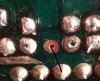
My question is - it looks like you can ground the tied together diodes as marked below by the black line (photo from ahess!). If I read one of the earlier posts correctly, this is in the ground plane.
If I was 100% confident I wouldn't ask, but as the VFETS are like gold it's best to ask.
.
(post edited for clarification.)
My question is - it looks like you can ground the tied together diodes as marked below by the black line (photo from ahess!). If I read one of the earlier posts correctly, this is in the ground plane.
If I was 100% confident I wouldn't ask, but as the VFETS are like gold it's best to ask.
.
(post edited for clarification.)
Last edited: