• The move to the new server is done. There are some software and database maintenance updates in process. This has us passing the hat around to help out. We appreciate any donations. Seriously, even a dollar helps. The payment page may be found here - https://www.audiokarma.org/support.html

SX-1250 Restoration

Did you measure the bias before changing any parts?
At the very least I would power up on DBT, then measure the bias. If it is high on DBT back it down, if it is low on DBT it may be OK. You did post it was working originally upon acquisition.
But, if you did not measure the bias before starting refurbishment, the last guy to set the bias may have been the guy that applied the unsanitary napkin. I would not be very trusting, and I would back it off before powering on again. You have little to lose by backing it off, and may toast some otherwise good parts if you don't . . . :dunno:
You are probably going to replace the bias pots anyway, right?
 
Unfortunately, I didn't get the bias measurements before replacing the caps. Lesson learnt!
Yes, the unit was working when I got it, although it runs warm on the R side (where the napkin'ed cap was).

Great suggestion to turn the pots down. Will do so. I should turn VR2 on power amp board CCW to back them off, right?
Yeap, got all new bias pots today also.
 
Last edited:
Unfortunately, I didn't get the bias measurements before replacing the caps. Lesson learnt!
Yes, the unit was working when I got it, although it runs warm on the R side (where the napkin'ed cap was).

Great suggestion to turn the pots down. Will do so. I should turn VR2 on power amp board CCW to back them off, right?
Yeap, got all new bias pots today also.
The SM says turn full CCW, so that is probably correct, if they are original. To be sure measure across them with an ohmmeter to verify 0Ω.
 
Alright, V2 on R was 188ohms and L was about 280ohms. Turn both CCW and get to about 0.5ohm on each.
Turned on and DBT passed. Two relay clicks!

Now onto the next step ... power supply board AWR-107-0 tonight.

Question for Mark
...
When should I rebuild the stabilizer board AWR-106-A?
Along with power supply board AWR-107-0 or together with protection board AWM-091?
I am also planning to switch out both S1 and S2 relays during protection board rebuild.

I also got a 500VA Variac off Amazon. Hope that is enough to handle 1250 going forward.
How much idle current is normal?

Thanks!
 
I am going to be a bit presumptuous and answer your AWR-106-A question, it should be done right after / along with the AWR-107-0. Once the AWR-106 (voltage regulator) is done and all the voltages are correct, then do the Protection board. You cannot be sure the protection circuit is working correctly until you are certain all the power supplies are right first.

I have an opinion about the Variac as well, though not everyone will agree. :eek: I don't believe a variac is very useful for solid state troubleshooting. While it does reduce input voltage, it increases available current by the same ratio, as it is a transformer: power in equals power out (minus internal losses). The DBT on the other hand limits both input voltage AND current draw, the more current draw is attempted, the more it drops the voltage, limiting available power dissipation in the unit under test to less than the wattage of the bulb. That being said, I wish I had a Variac for other purposes . . . :cool:
 
Hi Merlynski

Your inputs are equally appreciated. I just addressed Mark because he was the one provided the sequence.
What you have suggested makes total sense. I will do both 107 and 106 together tonight.

You also brought up a good point about Variac. I am planning to add current meter on it to see how much current is being drawn. However, this might be not as useful as DBT like you said to limit V and I.
I am just planning to use it to monitor during initial operation to make sure there is no latent failures lurking after a rebuild. Sort of like burn-in process ...
I hope this makes sense on variac.

Thanks again!
 
Recapped both AWR-107-0 and AWR-106-A. (transistors are not changed yet)
Brought it back up on DBT.
Passed and got two relay click. But now the S2 relay is making some buzzing noise for a min or two before it goes quiet. Both relays will be replaced anyway.
Measured Pin 17 on AWR-106-A around 63.5v and Pin 16 around -64v.
Will adjust them to SM 65v target after transistors are changed tomorrow.

I also did a pin out check for the replacement list provided by mattsd for AWR-106-A.
ALL of the replacements match original device pin out. Here is my cheatsheet.

I also notice that mattsd used -

Q10: 2SC945: 512-KSC2383YTA
Q11: 2SC945: 512-KSC1845FTA

Not sure why he used different one for Q11. Plan to follow his suggestion but not sure it is really needed.


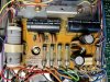
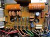
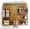
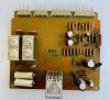
AWR-107-0 before and after

File_006.jpeg File_005.jpeg

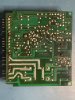
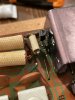
AWR-106-A before front and back. It seems there was some work done before.

File_003.jpeg File_004.jpeg


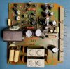
AWR-106-A after recap

File_002.jpeg

I found a couple of bad caps ...

File_000.jpeg File_001.jpeg
 
Q11 is the actual voltage regulator control transistor, the higher gain and speed of the KSC1845FTA make the regulator work better.
Q10 is used for current gain in the darlington configuration of Q10 and Q9. There the higher current, power dissipation, and SAO of the KSC2383YTA is more important. Those are the correct choices for that application.

I like your transistor 'cheatsheet', well done!

As for the current meter on the AC line, that is a good idea, but you do not need the Variac in line to use the current monitor. It just adds another variable in the test equipment. You can hit the power switch faster than you can turn down a Variac if the current goes crazy. I put a 5A circuit breaker in my DBT instead of the bulb when I am working on something I am 'worried' about protecting, just in case something lets go. It will (maybe) react faster than I can and I don't need to monitor the AC current. An AC current monitor IS on my list of things to build and add to my bench test equipment, though.
 
Last edited:
Replaced all active components and variable resistors on AWR-106-A.

A couple items I'd like to get confirmation -

1. Q6 2SA628A pin out

Internet (sorry that is all I have access to get information) showed that it is ECB. See below results. I also translated the Japanese version and they match.

2sa628-pinout.jpg
upload_2021-1-9_0-1-14.png

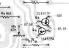
However, on the board, the pin out based on the orientation is BCE! I also tested the device and it aligned with the diagram! Also, the schematics agrees with the diagram on the board.

File_004.jpeg File_003.jpeg
upload_2021-1-9_0-6-23.png

So I placed the replacement to follow the device on the board. Please let me know if I am not correct.


2. Q2

According schematics Q2 should be 2SC869. However, on this board, it is 2SC1312. According to the list of lists, its replacement is KSC1845. But mattsd list has KSC2383. I follow his list. Please let me know if this is ok.
Based on the board diagram and tester, 2SC1312 is BCE. KSC2383 is ECB. So the replacement was installed in reverse.

File_001.jpeg

Board is all clean and ready to be plugged in. I also set the VR1 and VR2 to about 2.5k Ohm as the starting point.
I would like to confirm these two before I do so.
Thanks!

File_000.jpeg
 
According schematics Q2 should be 2SC869. However, on this board, it is 2SC1312. According to the list of lists, its replacement is KSC1845. But mattsd list has KSC2383. I follow his list. Please let me know if this is ok.
Based on the board diagram and tester, 2SC1312 is BCE. KSC2383 is ECB. So the replacement was installed in reverse.
Once again the mattsd listing is correct, Q2 is part of the darlington pair formed by Q1 & Q2. In that application the higher Ic and SAO is more important, so the KSC2383 is a better choice than the KSC1845. Q3 should be replaced with a KSC1845, as a better choice for that application.
Regarding transistor orientation, the PCB traces, component connections and circuit function are the final arbiter, regardless of what any documentation may say. It also is not unknown that a transistor may have lead order different than documentation. I test every transistor before I install it, to verify leads and function. Keep looking closely, you are doing it right!

In a voltage regulator circuit, setting the adjustment (VR1, VR2) to a center position is very reasonable for a starting position.
 
Last edited:
The KSC2383Y is a heavier-duty replacement for the 2SC1312. I can understand why it was recommended.

The Japanese translated pinout diagram does appear to differ from the other graphic you posted. Check carefully and orient accordingly.
 
Thanks Gents.
Plugged in and brought up slowly on DBT. It passed! Got two beautiful relay clicks .. :)
Pin 17 and 16 are measuring around +/-62v so I plan to keep at that level until protection board and power amp boards are restored.


Took out the protection board and finished the short list of upgrades. (Sad that new Omron is not made in Japan anymore but oh well ... )


Protection Board before and after

File_000 (7).jpeg File_001 (6).jpeg

In the process of upgrading S2 relay on the chassis.

I want to get input on the recommendation made by MTF regarding C11 and Q11 on power amp boards at this juncture. I am sure he has very legitimate reasons to recommend that so I would proceed with his direction.
But I wonder if I could go ahead and upgrade all other components along with C11 and Q11? I realize there aren't alot to replace anyway. I want to save removing and installing the output pairs so that I can save some time and mistakes during that process.

Thanks again!
 
You are most welcome!
C11 and Q11 on the power amp boards are part of the over-load detection circuit. If the transistor (Q11) gets leaky with age it causes false triggering of the protection circuit. It is a commonly seen failure. C11 desensitizes the circuit to high frequency, if it goes bad (it is an electrolytic) it can also cause problems with the over-load detection. It is commonly replaced with a film cap. A 505-MKS2C032201BKI00 0.22µF is a good option. I would upgrade all the transistors and electrolytic caps on the power amp PCBs.
 
You are most welcome!
C11 and Q11 on the power amp boards are part of the over-load detection circuit. If the transistor (Q11) gets leaky with age it causes false triggering of the protection circuit. It is a commonly seen failure. C11 desensitizes the circuit to high frequency, if it goes bad (it is an electrolytic) it can also cause problems with the over-load detection. It is commonly replaced with a film cap. A 505-MKS2C032201BKI00 0.22µF is a good option. I would upgrade all the transistors and electrolytic caps on the power amp PCBs.

Awesome! Thanks for the quick feedback. I will plow through both L and R side power amps today and tomorrow. I plan to set the VR2 on both L and R board to zero (CCW all the way before power up).
The unit has a lot of grime. So taking quite a bit of time cleaning and sanitizing it ... :blah:
 
Replaced recommended components on power amp boards as per mattsd list. Noticed that he only update Q1,Q2 and Q11. You recommended all transistors. It seems like I need to procure the rest of them since I went off to order his BOM list.
So I will bring up the unit again after reassembly at this stage to check for issue.

Found out that C11 has been changed to a film cap possibly by the napkin guy. Nonetheless, I upgraded to 5% WIMA cap. I also didn't have clean 220uF 16v cap but I found 80v cap that has at least similar ESR as the current one around 0.18 ohm. Plan to replace them during next phase when I upgrade the rest of the transistors.
I also noticed that Q11 2SC869 pin out is BCE on this board which matches 2SC1312 found earlier. Updated my cheatsheet.

I will set the VR2 all the way to CCW. I am not sure about the VR1 so I will set it somewhere in the middle.

Note to hobbyists - do not rely solely on the internet for pin out orientation of old parts.
I also found that having side by side images of before and after is not only useful for eye candy but also to do a quick sanity check. They enable you to do a comparison to see if something is off or not.

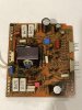
Power amp board AWH-048 before and after

File_000(1).jpeg File_001(1).jpeg
 
Part of the reason for my recommendation to do all transistors is my own OCD Perfectionism. Another reason is related to the first, 'since I am in there anyway' . . . Many will just do the ones that failed and/or appear on the "Worst transistor" lists, as some transistors have, historically, never had a problem. YMMV. Setting the bias adjustment to minimum makes good sense. Setting the dc offset to centered is just a reasonable starting point, especially if you changed the diff amp transistors.
 
Totally. I think the prerequisite for this hobby is to be OCD. :p

And here is my OCD, since I am there anyway, item today.

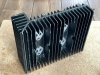
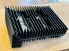
Heat Sink before and after

File_000 (8).jpeg File_001 (7).jpeg

Still got a couple more rounds of coating and baking to go before I get enough enamel on it but it is starting to look much better .... :D

As I have been OCD'ing the heat sink cosmetics, I haven't put together the boards yet. Hopefully I will get some time later tomorrow.
 
Put everything together and checked, double checked and triple checked all connections. Brought up on DBT, it passed with all new shiny components and got two heavenly-sounding relay clicks! :banana::banana::banana:
(New relays are so much quieter ..)

Adjusted the VR1 and VR2 on stabilizer board to get +/- 65v. Plan to adjust the power amp board DC bias after hacking some 5.1k ohm load connections. After that, will give the unit a few days of testing/usage before proceeding to the front end of the unit. Any concerns?

Output transistors Before and After ( R channel )

File_001.jpeg File_002.jpeg

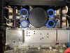
With all boards in place ..

File_007.jpeg

VR1 and VR2 adjusted
File_004.jpeg File_005.jpeg
 
Last edited:
Totally. I think the prerequisite for this hobby is to be OCD. :p

And here is my OCD, since I am there anyway, item today.

Heat Sink before and after

View attachment 2093467 View attachment 2093468

Still got a couple more rounds of coating and baking to go before I get enough enamel on it but it is starting to look much better .... :D

As I have been OCD'ing the heat sink cosmetics, I haven't put together the boards yet. Hopefully I will get some time later tomorrow.

Looks good.
I hope you masked off the heat transfer surfaces for the output transistors, and didn't paint them...
 
Last edited:
Back
Top Bottom