• The move to the new server is done. There are some software and database maintenance updates in process. This has us passing the hat around to help out. We appreciate any donations. Seriously, even a dollar helps. The payment page may be found here - https://www.audiokarma.org/support.html

Yamaha CA 600 Repair 2026

I just ordered a few MJE253 transistors, they won't be here till next week.

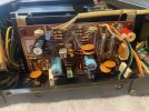
Please look at this picture. Of the two circled transistor mounting holes. Please tell me where the Emitter goes. From what you guys taught me in the top one (TR611) it goes in the top hole. In the bottom mounting (TR609) the emitter goes in the bottom hole. IS THAT CORRECT?

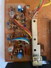
In the second picture you can see the factory board before I started working on it. Both TR611 and TR609 transistor point upwards with their lettering facing upwards. To me it means both Emitters are on the far right in this picture which contradicts the schematic arrow drawings on the board in pic1 of TR611.

What am I not understanding here?
 

Attachments

  • 85a4d728-3e66-4d85-b32c-bd8eb87a4202.jpg
    85a4d728-3e66-4d85-b32c-bd8eb87a4202.jpg
    234.8 KB · Views: 8
  • 2f0b0ed4-2669-45a0-a849-b667cb212e39.jpg
    2f0b0ed4-2669-45a0-a849-b667cb212e39.jpg
    128.9 KB · Views: 8
Last edited:
The way they have it drawn is a little obscure and not clear. hard to do on silk screens.

55536148596_934b485660_o.jpg


For the top Transistor, fr the bottom transistor the arrow for the Emitter is at the through hole .
55536325764_edd433eabc_b.jpg
 
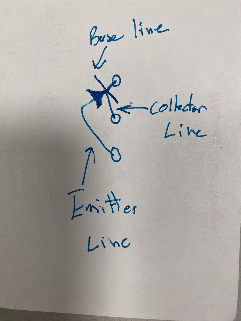
So if the arrow is pointing directly at a through hole, then it is the Emitter OR away from it and is blocked by a line (the base line) then it is also the Emitter?

Like in my drawing? Is that correct?

I hate you guys.
 

Attachments

  • 597cf3cc-72c8-4b1c-a536-a6dc1eb7c4e6.jpg
    597cf3cc-72c8-4b1c-a536-a6dc1eb7c4e6.jpg
    84.5 KB · Views: 3
Last edited:
So if the arrow is pointing directly at a through hole, then it is the Emitter OR away from it and is blocked by a line (the base line) then it is also the Emitter?

Like in my drawing? Is that correct?

I hate you guys.
Your drawing is correct , see that you are learning !!!

if two lines come off the Base line its either a collector( no arrow) or an emitter ( with Arrow) , a single line is off the Base line is the base.

EDIT: A little more info for you, an arrow toward base is a PNP , arrow away from base line is a NPN .
 
I just ordered a few MJE253 transistors
If you are wanting to replace TR611 then you should also consider replacing its compliment TR609. I'd also be asking if MJE253 is a suitable sub for driver duties, I'm very poor in this area so will leave that to others

edit Is TTA004B and TTC004B overkill or just wrong?
 
Last edited:
If you are wanting to replace TR611 then you should also consider replacing its compliment TR609. I'd also be asking if MJE253 is a suitable sub for driver duties, I'm very poor in this area so will that to others
What is TR611 original, I don't have that schematic download on my work computer

nashou
 
Gentlemen,

Nashua66 - can I get a clarification on what this means? (if two lines come off the Base line its either a collector( no arrow) or an emitter ( with Arrow) , a single line is off the Base line is the base)

MBZ - I have some extra KSC2690's I can replace TR609 and planned to because they got pretty hot at one point. MJE253 is what I used in the TR611 spot and what I ordered this morning to replace the bad one.

In my opinion, whether it is a PNP or an NPN is a waste of space to be marking it on the printing on the board. What could it matter if it is an NPN or a PNP as long as you are using the correct transistor and if it has the same PINOUT as the original and you know which through hole is the Emitter hole that is all the matters.

What I mean is if you remove a 2SA682 and are replacing it with a MJE253 then it is going to be correct because they do not make an NPN and a PNP MJE253, they only make a PNP MJE253. And if you are putting an NPN in that spot then you have already made a crucial mistake. There is only so much room to print on the board, why does that need to be on there when its already in the SM schematic?


This damn thread is 6 pages long now, WTH!
 
What I mean is if you remove a 2SA682 and are replacing it with a MJE253 then it is going to be correct because they do not make an NPN and a PNP MJE253, they only make a PNP MJE253.
The MJE243 is the complimentary

I have some extra KSC2690's I can replace TR609 and planned to because they got pretty hot at one point. MJE253 is what I used in the TR611 spot and what I ordered this morning to replace the bad one.
For amp stability, I would be replacing the driver transistors(TR609, 611) with a complementary pair.
Either MJE243 & MJE253
or TTA004B & TTC004B <= my choice or KSC2690/KSA1220 if you can source
 
my Excel Spread sheet says either a KSA1220 or a MJE253G.
the KSA's aI believe are no longer available.
Yeah, i saw that. Was thinking the higher capacitance of the MJE's would make them not "ideal" thinking the TTA/TTC004B's would be slightly better.

Maybe add another sheet on your xl to included suggested VAS/Driver/Output transistors, ie, purpose built VAS etc that are still available today. Add diff pair?? KSA992/KSC1845?
 
I am still confused on the ECB diagram.

In these 3 pictures all transistors are ECB and all in a TO-92 body.

TR404 and TR406 should be facing the same way as TR408 because all three symbols are exactly the same. TR407 TR405 and TR403 are the same story, the 3 symbols look the same and are oriented in the same direction so all 3 transistors will be facing the same way. But this is not how they came out.

Now in the photo of TR401 and TR402 the arrow is pointing at the through hole at 9:00 (will be the emitter hole) so both of these transistors will be facing down in the picture?
 

Attachments

  • 406 adn 404.jpg
    406 adn 404.jpg
    113.3 KB · Views: 11
  • 403 and 405.jpg
    403 and 405.jpg
    104 KB · Views: 10
  • 401 and 402 .jpg
    401 and 402 .jpg
    123.3 KB · Views: 10
OK, so we are now looking at the function board @#$%!

First up errors do occur with those transistor icons, that's why before pix are recommended.
The icons clearly show the emitter, insert the emitter leg in the relevent hole...

Assuming the icons are correct
TR404 and TR406 should be facing the same way as TR408 because all three symbols are exactly the same.
Yes, correct

TR405 and TR403 are the same story, the 3 symbols look the same and are oriented in the same direction so all 3 transistors will be facing the same way.
No, TR403 and TR405 should be facing to the right towards the blue, green white wires

Now in the photo of TR401 and TR402 the arrow is pointing at the through hole at 9:00 (will be the emitter hole) so both of these transistors will be facing down in the picture?
Correct
 
@PioneerPro do you own a cheap parts tester that tells you what transistor you have? Its possible the ones you pulled out had a different
pin out config, also when removing the parts document the part you pulled out , its location and orientation on the board along with detailed pics of the face of the transistor and pics from above as well.

s-l1600.jpg
 
Yeah, i saw that. Was thinking the higher capacitance of the MJE's would make them not "ideal" thinking the TTA/TTC004B's would be slightly better.

Maybe add another sheet on your xl to included suggested VAS/Driver/Output transistors, ie, purpose built VAS etc that are still available today. Add diff pair?? KSA992/KSC1845?
I keep forgetting about the TTA/TTC parts, also there are the KTA/KTC parts from KEC corp I need to start looking at.

Regarding that spread sheet I don't know who originated it but I downloaded it and as parts became unavailable and i come across them in the spread sheet I try to put in any newer parts that would work over the latest end of life parts. Im not an expert but I try ;) So this info you gave is just what I need.

Athanasios
 
OK, so we are now looking at the function board @#$%!
I understand but I am waiting on parts so had time to kill. Why not just double check everything and make sure it it correct. Also I do take pics before I start workng on anyboard and I draw a diagram.

No, TR403 and TR405 should be facing to the right towards the blue, green white wires
Actually this one was correct also, it was just hard to see because I chopped off in the photo TR407 but it was facing right also. Here is a better pic.


Nashua66 - No I do not own a parts tester because I don't do much of this work. I do enjoy working on electronics and it is quite satisfying but I have no formal training.

MBZ - Here is a photo of the function board all done.
 

Attachments

  • 164ae062-6142-42e7-9e24-dc0c6c5f697c.jpg
    164ae062-6142-42e7-9e24-dc0c6c5f697c.jpg
    130 KB · Views: 4
  • 2f569b99-0b36-459c-bc53-c97cac64149c.jpg
    2f569b99-0b36-459c-bc53-c97cac64149c.jpg
    129.4 KB · Views: 4
Nashua66 - No I do not own a parts tester because I don't do much of this work. I do enjoy working on electronics and it is quite satisfying but I have no formal training.

MBZ - Here is a photo of the function board all done.
Its cheap, 14 buckaroos , it will save you time giving you more tim to play with your wife Nice can's ;)
Buy a tester that will save you time and money. You can buy it for a few bucks.
Pavel;)
Yep cheap and saves time I have like 4 of them just incase ;)

nashou
 
I have nothing to do while I wait for the new TR609 and TR611 transistors to come in so I installed a brand new KSC2690 in the left board and used the newer MJE253 from the right board in the left board to make that Main Amp Board fully operational.

I ran a DBT with the fuses in and no light
I ran a DBT with the can output transistors in and still no light. All seams well for now.

I measured Vdc at TP1 and got .28volt. I repeated at TP2 and got the same .28volt. And just for the hell of I I measured Vdc between TP 1 and TP2 and got .03volt.

Then I did the red, blue, green, purple, test from earlier and here is what I got.

Red 1.43v
Blue .88v
Green -0.30v
Purple -0.30v


This link will show you were these points are on the board.

 
Back
Top Bottom