• The move to the new server is done. There are some software and database maintenance updates in process. This has us passing the hat around to help out. We appreciate any donations. Seriously, even a dollar helps. The payment page may be found here - https://www.audiokarma.org/support.html

Pioneer M-90 Issue- need help.

Mouser has a few of each with different suffix letters. Does it matter which I choose and should each of the 2 have the same suffix?
the suffix in ( ) seems new, might have something to do with the "country of" assembly/diffusion/origin drama and supply chain sabotage currently being inflicted by a particular country. further research is needed.

on mouser you can select multiple components in the search list for side-by-side spec comparison.

Screenshot 2026-05-10 at 22-30-54 Compare Products - Mouser Electronics.png

for some transistors the suffix indicates the range of hfe which can be important. an example for the 2sc5200 would be -R and -O from what is specified in the datasheet. reading through spec sheets can be a headache but it is helpful to know that the correct physical size / pin configuration: ecb ebc / electrical parameters are being purchased or considered.

*looks like 2sc3907p is the norm for the amp. inchange semi vs toshiba may or may not have a significant difference in regards to build quality.

*the 2sc5200 is indeed a more robust component vs original. the unit cost is low enough that comparison shopping for an even higher spec component might be futile.

benefits of a higher spec output transistor is simple, better longevity and less stress at normal and extended output amplitudes and thermal derating performance.

Doesn't appear that any of those are available. Is there a spot on AK somewhere that shows available crosses for transistors?
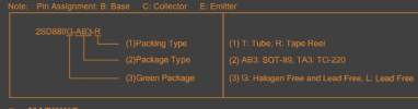
searching for part number is a good starting point on ak. there are various audio forums with equally useful content/info as well.

Screenshot 2026-05-10 at 22-57-27 ds.pdf.png

using the 2sd880 as a random example, there are some spec sheets available. and for vintage gear thats a plus, some components are almost non-existent when searching for basic specs.


if i dont find a suitable part number equivalent within about 10-30minutes of searching then its mouser spec shopping for a suitable over-kill component which i end up doing more often than not.


there is also a top 10 list of faulty transistors on ak that has grown over the years which also specifies a suitable upgrade/replacement device.
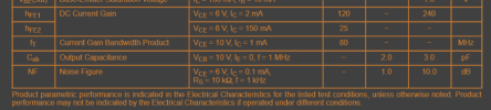
 
something to watch out for as well, if specification shopping/comparing, would be if a transistor has "noise figure" spec. they can be difficult to find an upgrade due to wattage limitations and Vce parameters.

Screenshot 2026-05-11 at 22-14-46 KSC1815 - NPN Epitaxial Silicon Transistor - KSC1815-D.pdf.png

a popular replacement/update/upgrade example would be the above ksc1815. just one of many out in the active inventory market.
 
something to watch out for as well, if specification shopping/comparing, would be if a transistor has "noise figure" spec. they can be difficult to find an upgrade due to wattage limitations and Vce parameters.

View attachment 3760506

a popular replacement/update/upgrade example would be the above ksc1815. just one of many out in the active inventory market.
Appreciate all the information! What I decided to do was search for original replacements for the predrivers off pins 9 and 13 of the chip- Q119 thru Q126. Found on eBay what are advertised as original Toshiba transistors- 2SC2705, 2SA1145, 2SC2238 and 2SA968. Also orederd replacement power transistors from Mouser: 2SC5200 and 2SA1943. I went with the OS1F suffix since I could get both transistors with the same suffix and phisical size and lead length looked good.
 
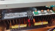
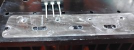
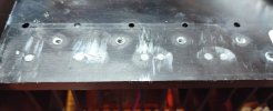
So, I made a rookie mistake. Assumed the recommended replacements for the power transistors were the same case size as the originals, so when I was checking data sheets, I only looked at lead length and spacing- not case size. Doh! They'll fit, but it will take some modification. There're some pins through the surface of the heatsink used to hold the mica insulators in place. Will have to sheer those off so the new transistors will lay flat against the heat sink. You can see in the one photo I've already cleared on of them. I hope this is worth the effort.
 

Attachments

  • X Size.jpg
    X Size.jpg
    77.1 KB · Views: 7
  • X Fit.jpg
    X Fit.jpg
    75.5 KB · Views: 7
  • X Sheer.jpg
    X Sheer.jpg
    52 KB · Views: 7
the larger outputs should help with thermal longevity (significantly) and kick dynamic response up a notch or two depending on how much juice the speakers can handle.

the originals might be worth saving for future projects or amps with undersized factory transistors.

definitely be careful when sourcing anything on ebay, it can be a gamble regardless of the sellers rating and buyers feedback (like amzn 5-star lawsuit/drama).
 
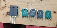
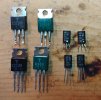
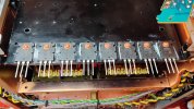
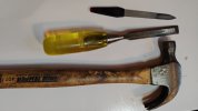
A bit of progress. A pic of one channel's old and new pre-drivers- the replacements I got from a few ebay sellers that, at least, look legit :rolleyes: A closeup of the studs I had to sheer off and file down for the bigger transistors to lay flush to the sink along with the tools I used. Also picked up some TO-3P mica insulators to fit the new transistors. Now to solder them in and move to the other side.
 

Attachments

  • IMG_20260521_180053330_HDR.jpg
    IMG_20260521_180053330_HDR.jpg
    104.9 KB · Views: 11
  • IMG_20260521_180045228.jpg
    IMG_20260521_180045228.jpg
    53.3 KB · Views: 10
  • IMG_20260521_173533824_HDR.jpg
    IMG_20260521_173533824_HDR.jpg
    89.1 KB · Views: 9
  • IMG_20260520_175647154.jpg
    IMG_20260520_175647154.jpg
    49.5 KB · Views: 11
  • IMG_20260520_175129986.jpg
    IMG_20260520_175129986.jpg
    126.3 KB · Views: 14
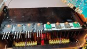
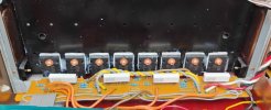
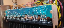
The original power transistor leads were bent at a right angle to line up with the PCB. Since the new transistors are larger, the bottom end sits lower on the heat sink requiring a bit more lead manipulation but noting too difficult. First side done and a pic of the old added for comparison.
 

Attachments

  • Power Trans.jpg
    Power Trans.jpg
    84.5 KB · Views: 16
  • IMG_20260524_094455361_HDR.jpg
    IMG_20260524_094455361_HDR.jpg
    64.7 KB · Views: 11
  • IMG_20260524_094302997_HDR.jpg
    IMG_20260524_094302997_HDR.jpg
    85 KB · Views: 10
  • IMG_20260523_084152912.jpg
    IMG_20260523_084152912.jpg
    75.6 KB · Views: 12
  • IMG_20260523_084209063_HDR.jpg
    IMG_20260523_084209063_HDR.jpg
    77.8 KB · Views: 16
the larger outputs should help with thermal longevity (significantly) and kick dynamic response up a notch or two depending on how much juice the speakers can handle.

the originals might be worth saving for future projects or amps with undersized factory transistors.

definitely be careful when sourcing anything on ebay, it can be a gamble regardless of the sellers rating and buyers feedback (like amzn 5-star lawsuit/drama).
So, before I put in the replacement pre-driver transistors, I checked them all on my tester and they all looked good. Once I got the power transiters installed I checked them with the diode tester on my fluke and there were no issues. Also checked to make sure there were no shorts between the heat sink and the collectors of those transistors. When it wouldn't come out of protection on the DBT I gave the unit a good hard look to see if I crimped a wire or messed up a solder joint and I couldn't find anything. So, not knowing if the pre-drivers were legit, I put the originals back in, but no change. I also retested those replacements again, and they checked the same on the tester. Don't really want to pull this off the DBT to see what happens or to check voltages. Is it possible it's just not happy with those replacement power transistors?
 
dc offset and bias might be outside of normal parameters and the protection circuit is responding accordingly.
 
dc offset and bias might be outside of normal parameters and the protection circuit is responding accordingly.
So, you think it possible those alternates might cause that? Looking for a little assurance before I go through the ass pain of going back vs looking elsewhere : )
 
when changing out complex devices like transistors, and in critical locations as it pertains to an audio amp, there is a high probability that certain calibrations will need to be re-calibrated i.e. dc bias if any of the outputs are replaced.

since the protection circuit triggers due to certain conditions, possibly explained in the service manual (i havent looked yet), and the system functioned stable prior to upgrading the outputs the list of suspects is quite short.

the chances that one original output transistor has the exact same hfe and electrical parameters as the new replacement is effectively zero, now times that by however many outputs were replaced.

logically i would do the offset and bias measurements even if by some infinitesimal chance they are still correct or within normal range. the joys of assembling and disassembling a system soon becomes second nature... and possibly a reoccurring theme of ones nightmares.
 
actually scratch that... i am still thinking that the bias and offset can be adjusted in the first place. this system uses a central chip.
 
if all the replacements have no ecb/bce/ebc pinout issues then it would be a good idea to revisit chip pinout measurements once again. what wattage dim bulb is being used vs when the amp was stable and on dim bulb?
 
if all the replacements have no ecb/bce/ebc pinout issues then it would be a good idea to revisit chip pinout measurements once again. what wattage dim bulb is being used vs when the amp was stable and on dim bulb?
Quick update. Put all original transistors back in, although not all in the exact same spot they were originally in. I checked them all as well. Unit still stuck in protection mode after that. After a lttle tinkering it turns out it was likely a bad connection with J3 on Pwr Amp-A PCB and/or J4 on Pwr Amp-B PCB and now it's out of protection and very little current draw. The rail voltage looks good and the +/- 3VDC on the chips look close, but the L-Ch bias voltage on the chip is not right. Haven't really dug into it to figure out what it might be. Wondering if I should direct solder the ribbon cables as those jacks aren't the easiest to work with and don't seem solid. The J3 connector clamp is broken as well. Alaso wondering if I should go back to the new transistors and see what that does, although with all the originals looking good on the tester I don't think that it will correct the current issue.
 
bad connections can crop up more and more with the moving of boards. vintage gear notoriously bad in regards to wiring/connection issues while trying to repair something.

with the swapping of parts be careful not to thermally stress or wipe out pads/lands/traces. a slight fracture can be difficult to track down.

direct soldering wire wrap connections and connectors is beneficial.
 
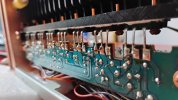
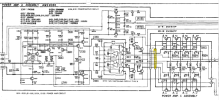
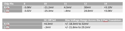
Bingo! I don't think my issue was J3/4 mentioned above. It was J2 between the left channel Amp-B and Amp-D PCBs. Specifically on the Amp-D side. It's a 9-pin ribbon cable soldered on both ends but on the Amp-D, side most of the solder joints were bad along with solder joints on a few other wires going to that board. I thought for sure I checked all that when I was replacing all the fusible resistors, but I guess I missed this one. Wish I'd caught that earlier as it would saved a lot work and heartache. Anyway, after squaring all that the left channel bias voltage is just about spot on across the 8 power transistors. Still a slight issue on the right. On the R-Ch IC: pin 8 -3.18VDC and 14 +3.21VDC. Calling those good, but pin 10 is -19.5mv and pin 12 is +28.5mv when they should both be 25mv. Going to look at my chip tables and see if one of the replacements I found aligns closer to the current left channel chip.
 

Attachments

  • Ribbion Cable.png
    Ribbion Cable.png
    222.6 KB · Views: 2
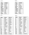
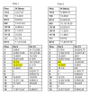
Well, the charts didn't help. The original chips (currently installed) are closely matched to each other (1st attachment below) as well as the replacements I got (second attachment). However, comparing the original chips to the replacements it looks like completely different sets of chips. I did notice the DCV readings I have now for both channels match where I was on my May 6 post which leads me to believe the J2 ribbon cable was likely the cause of my original hum and high left channel high bias all along. There is a bit of a difference between the original L/R channel chips on the resistance readings for pins 1 to 9 and 1 to 13. Could that be a culprit for the off bias readings on the R-Ch? Is it off enough to worry about?
 

Attachments

  • Chip Readings.png
    Chip Readings.png
    73.9 KB · Views: 1
  • Chip Readings (2).png
    Chip Readings (2).png
    74.3 KB · Views: 1
Last edited:
So, I tried swapping the original chips I had installed- right to left and left to right. A bit of a change but not much so likely not the chips causing the off readings. For reference, pins should read: 8=-3.3V, 10=-25mV, 11=0V, 12=+25mv, 14=+3.3V. All DC. Is it worth chasing this down? Should I consider trying the new power transistors or leave it be?

1780611306010.png
 
Could that be a culprit for the off bias readings on the R-Ch? Is it off enough to worry about?
some circuit and chip variances will make things less than perfect (hence +/- 5% or 10% is a tolerable tolerance). resistance measurements on the chip pins helps with looking for unusually low resistances (shorted internally or low resistance) and considered to be a crude/low-level component test (still useful though). in terms of overall chip functionality, only in a circuit with power applied and design spec load connected will it show if it works or not (multi-pin mystery box).

Is it worth chasing this down? Should I consider trying the new power transistors or leave it be?
are the numbers with or without dim bulb and is there a load connected?

the numbers in post-119 are the original outputs (power transistors)?
 
Back
Top Bottom