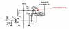
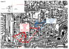
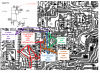
This is, it seems, kind of a redundant sensor scheme to sensor A. The unusual thing I already see, the signal is pulled off at op-amp Stage 2 which is still kind of noisy. The transistor stage is, I guess, an input buffer. I had to go refresh my transistor understanding. I always liked vacuum tubes, it always seemed kind of straightforward. Transistors, while more-or-less the same, somehow always escaped me a little bit.
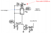
The transistor is in a common emitter configuration. The load line is constructed by locating the supply voltage on the x-axis (5V) and the collector current (equal to supply voltage divided by the load resistor (5V)/(3300ohm) = 1.5mA
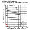
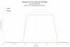
Weird place to locate the load line. I’m, pretty sure this will be an on-off transistor configuration rather than a linear amplifier. Common emitter will also invert the signal. So the input to the transistor somes from Stage 2 which is mostly a noisy 0 to 3V with spikes at the record lead-in, gaps and lead-out that are up to 12 to 14V. See below for what the output from Signal E Stage 2 looks like.
Note that as a voltage spike occurs at the input to the transistor, the transistor base starts to conduct. This causes the transistor collector to emitter to conduct (resistance collector to emitter goes down). The collector, also known as the output, now approaches the voltage more toward the ground side of the transistor rather than the supply side. So yes, signal inversion, high input signal equals low output signal. When the signal coming in is low or near zero, the signal out will be high, near the max of the supply to the transistor. In other words, +5V. And our spikes that we want to recognize? Spikes down from +5V to 0V. This signal is then fed in to the multistable multivibrator IC9a, pin5.
Now, here is an interesting twist. Ain (pin4) is grounded (low). The signal goes in to Bin (pin5). The IC is looking for a high to low transistion at pin B in order to output a pulse. So yes, it is correctly looking for an inverted signal as presented by the transistor. Output comes out of IC9a pin6, the regular, not the inverting output. So we should get a pulse out from low (0V) to high (+5V) for 0.45sec. The pulse is sent to the MPU, pin3, input PC1).
Why do I propose a summer intern? First, picking off the noisy signal at Stage 2 seems questionable. Maybe Stage 2 output is not supposed to be so noisy? Well, I said before, that is one to watch. Maybe the phototransistors have aged and are just noisy.
This transistor input design line is also suspicious and looks really sensitive. It seems to me it will either react to the smallest signal (noise) and stay in the conducting state all the time or just the opposite, it will slam against the other extreme and stay non-conducting all the time. And lastly, all the inversion. Well, it’s available on the chips, I guess. Just confusing and, with logic tables, it can get a little dicey.
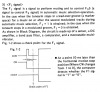
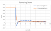
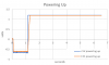
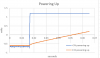
The interesting part? Vinyl record size identification seem to be working OK. The system seems to be finding the record start relatively well. I think there’s a reason for this that you’ll see later when you see the actual signal traces. The E3 sensor signal looks like it is slamming to the high side (+5V) most of the time. In this state, it does not overide Sensor A (located underneath the tonearm), and in fact, defers to Sensor A to initiate the tonearm drop onto the record start. In essence, it is not really used.
Here's what things are really doing:
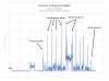
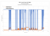
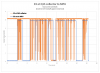
So, E3, mostly at +5V, mostly doing nothing to inhibit Signal A from finding the record start.