

You are using an out of date browser. It may not display this or other websites correctly.
You should upgrade or use an alternative browser.
You should upgrade or use an alternative browser.
Sansui Turntable - Particularly XR-Q11


mootej
Active Member
Sensor F
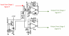
The Sensor F signal comes from Stage 1 and splits in two. The first path goes through a transistor with an adjustable (VR2 “F2 Sensitivity Ad.”) input, then on to a Stage 2 op-amp. We’ll call this path and signal “F2”.
The second path goes directly to a Stage 2 op-amp. We’ll call this path and signal “F1”.

I'll try to attach component datasheets for the transistor Q10 (2SC945), the infamous “shoot on site” diodes D9, D10 and D11 (VD1212) and the other diode D12 (1S2473D).
Again, the suggested replacement scheme for the VD1212’s, if you need or want to replace them: use two 1N4148’s in series. And the 1S2473, if it needs replacing, use 1N4148.
The Sensor F signal comes from Stage 1 and splits in two. The first path goes through a transistor with an adjustable (VR2 “F2 Sensitivity Ad.”) input, then on to a Stage 2 op-amp. We’ll call this path and signal “F2”.
The second path goes directly to a Stage 2 op-amp. We’ll call this path and signal “F1”.
I'll try to attach component datasheets for the transistor Q10 (2SC945), the infamous “shoot on site” diodes D9, D10 and D11 (VD1212) and the other diode D12 (1S2473D).
Again, the suggested replacement scheme for the VD1212’s, if you need or want to replace them: use two 1N4148’s in series. And the 1S2473, if it needs replacing, use 1N4148.
Attachments

mootej
Active Member
No more XR-Q11's to ever go to the island of misfit toys...that's the hope, @Watthour . Hey, I saw in another thread that you lost some electrons and were hoping to find them again with an SEM... if they are Auger or photoelectrons, I can probably help locate them. If they are just regular old electrons, there probably just phonons now.
mootej
Active Member
Let’s look at the more complicated F2 Stage 2 circuit:

Lots going on here. First thing is a variable resistor VR2 on S-0053, the main board. The voltage we’re seeing out of signal F Stage 1 is 0 to 5V. VR2 allows us to pick off as much or as little voltage as we want and feed it to transistor Q10. We can monitor this voltage at TP7. Here’s the procedure for setting it.

I haven’t yet performed this procedure, I don’t have the little plastic adapter or a cartridge/needle, so for the moment, we’ll just go with where VR2 is set.
I believe the engineers put this transistor amplifier stage to help with the following: When the tonearm lifter is up, the phototransistor sees less signal than when the lifter is down. But we’ve already adjusted the signal from Stage 1 to 5V with the lifter up when it is over a gap in the music on the vinyl. In this procedure, we put the lifter down on the gap and use VR2 on S-0053 to back off the voltage with the lifter down. Apparently, this is only required for signal F2. Indeed, F2 is the only signal that is assessed while the tonearm is down. The rest of the signals are only assessed while the tonearm is up.
Note that this VR2 adjustment might be a little confusing since there is more than one “VR2”. The Sansui engineers started labeling everything from “1” for each circuit board. I get it, if you have independent teams designing various parts, the team starts at “1” and the teams don’t need to coordinate labeling, just inputs and outputs. Just be careful as an end-user 45 years later that you get the correct VR2, the one on the main circuit board, not the sensor circuit board or some other auxiliary board!
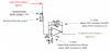
The transistor, Q10, looks like a common collector configuration, typically a buffer circuit that has a gain of about 1, a voltage follower, where voltage out is about the same as the voltage in. It has one difference. There is a diode in the emitter circuit. I think this will have the effect of requiring a voltage input of at least 1.3V, effectively filtering out any signal below 1.3V. So it looks like we were correct, the voltage follower along with VR2 allows us to dial down the input just a little bit. It should also filter out any low level background.
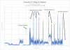
Here are the voltage scans of several of these points along the way…
1. input voltage from the previous stage (signal F Stage 1)
2. voltage after VR2, the input to Q10
3. The emitter at Q10, a point prior to the diode
4. The input to the next stage, a point after the diode.


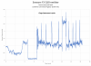

With VR2 set where it was, the circuit is definitely dialing down the signal by about 40%. And, once again, the diode-filtering is ok, but not great. Just like before, the background record-groove signal looks a little high for this diode filtering to work. Same situation as the diode filtering between Stage 1 and Stage 2 for signals E and F1. Again, interesting, but for the moment, let’s assume it’s ok.
Lots going on here. First thing is a variable resistor VR2 on S-0053, the main board. The voltage we’re seeing out of signal F Stage 1 is 0 to 5V. VR2 allows us to pick off as much or as little voltage as we want and feed it to transistor Q10. We can monitor this voltage at TP7. Here’s the procedure for setting it.
I haven’t yet performed this procedure, I don’t have the little plastic adapter or a cartridge/needle, so for the moment, we’ll just go with where VR2 is set.
I believe the engineers put this transistor amplifier stage to help with the following: When the tonearm lifter is up, the phototransistor sees less signal than when the lifter is down. But we’ve already adjusted the signal from Stage 1 to 5V with the lifter up when it is over a gap in the music on the vinyl. In this procedure, we put the lifter down on the gap and use VR2 on S-0053 to back off the voltage with the lifter down. Apparently, this is only required for signal F2. Indeed, F2 is the only signal that is assessed while the tonearm is down. The rest of the signals are only assessed while the tonearm is up.
Note that this VR2 adjustment might be a little confusing since there is more than one “VR2”. The Sansui engineers started labeling everything from “1” for each circuit board. I get it, if you have independent teams designing various parts, the team starts at “1” and the teams don’t need to coordinate labeling, just inputs and outputs. Just be careful as an end-user 45 years later that you get the correct VR2, the one on the main circuit board, not the sensor circuit board or some other auxiliary board!
The transistor, Q10, looks like a common collector configuration, typically a buffer circuit that has a gain of about 1, a voltage follower, where voltage out is about the same as the voltage in. It has one difference. There is a diode in the emitter circuit. I think this will have the effect of requiring a voltage input of at least 1.3V, effectively filtering out any signal below 1.3V. So it looks like we were correct, the voltage follower along with VR2 allows us to dial down the input just a little bit. It should also filter out any low level background.
Here are the voltage scans of several of these points along the way…
1. input voltage from the previous stage (signal F Stage 1)
2. voltage after VR2, the input to Q10
3. The emitter at Q10, a point prior to the diode
4. The input to the next stage, a point after the diode.
With VR2 set where it was, the circuit is definitely dialing down the signal by about 40%. And, once again, the diode-filtering is ok, but not great. Just like before, the background record-groove signal looks a little high for this diode filtering to work. Same situation as the diode filtering between Stage 1 and Stage 2 for signals E and F1. Again, interesting, but for the moment, let’s assume it’s ok.
Last edited:
mootej
Active Member
Oh, the other part @Watthour , it would also be nice if I found out what was wrong, fixed it and it worked. I've got to admit, though, I'm really enjoying the winter project of figuring out how they designed this, piece-by-piece. It's been an awesome journey so far.Very well done, and great documentation. This is probably now the definitive resource on XR-Q11 service.

mootej
Active Member
Last Stage for the op-amps: Stage 3, the Comparators. Here the functional diagram:
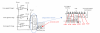
First, signal E is split in two. The signal from Stage 2 is split out as a separate signal, “E3”. The signals from Stage 2 (E, F1 and F2) also head into the non-inverting input of the Stage 3 op-amps.
There are a set of reference voltages produced by a resistor voltage divider network connected between +18V and ground. The reference voltage is selected and sent to the comparator op-amps with a triple-pole-double-throw switch. With the switch, the user can select H/M/L for the track sensor sensitivity. Apparently, depending on the way the master record was prepared, the track gaps in the vinyl can be more/less reflective. And, as with any engineering problem, we are performing a balancing act between sensing a track and triggering on noise. To give the [likely…] high-end user of this turntable a vent for their angst when track selection does not work as planned and a compromise solution for the engineering team, they installed the sensitivity switch. The switch picks off a voltage to feed into the comparator inverting input. The comparator will then only see:
- low setting – signals above 11 or 12V,
- medium setting – signals above ~6V or
- high setting – signals above ~4V.
The comparator adds the voltage from the signal, subtracts the reference voltage (e.g. senses the difference), performs any amplification and filtering based on the feedback and finally, outputs the difference. Any difference at the output above a certain positive voltage is shunted to ground by the Zener diodes Dz1, Dz2 and Dz3. The datasheet for the Zener diodes is attached...they cut off the voltage at 4.5 to 5V.
For filtering, the bandwidth on Stage 3 is pretty wide (something like a bandpass of 10Hz to 1KHz). Most of the frequency filtering was performed at Stage 2. As for amplification, it’s pretty high since we really want this last stage to act as an on-off switch (the gain is probably somewhere near 500). So, the circuit looks like it is set up to go all out (2V less than the supply of 18V, according to the datasheet) when there is a signal AND to cut off to zero anything at the input below the voltage set by the sensitivity switch. Then, the Zener diodes limit the output to 4.5 to 5V.
Once again, here’s the test procedure I use to generate the signal traces:
1. I hook up the test point of interest to the oscilloscope positive lead,
2. The negative lead is attached to TP2, a ground,
3. I plug in and turn on the turntable,
4. I set the speed to 33-1/3rpm,
5. I use a 30-cm diameter record with 5 tracks, a lead-in gap, a lead-out gap and four gaps between the songs,
6. I push song selection “7” so the tonearm will lift, go all the way to the lead-out track, determine there are not 7 songs and return the tonearm to the rest, amd
7. The signal from the sensors will be continuous and see first the plinth, then the edge of the platter, the lead-in gap, the grooved and gap tracks, the lead-out gap and then the reverse of each as the tonearm returns to the rest.
Here’s the output for the Stage 3 signals:
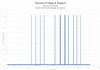
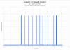
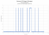
Note the sensitivity switch was set on High. Everything seems to be working or at least we’re getting the off-on behavior and the max signal behavior we expect. There may be a spurious signal here and there, but in general, things look pretty much OK.
So no smoking gun yet! Not sure why it's not working...at this point, I would put my money on some kind of timing issue with the signals.
On to the next section, defined in the functional diagram as the monostable multivibrators…intended to provide a known pulse amplitude and duration to the MPU. And some delay circuits to match up the signals for the lead sensor, the trailing sensor in time.
First, signal E is split in two. The signal from Stage 2 is split out as a separate signal, “E3”. The signals from Stage 2 (E, F1 and F2) also head into the non-inverting input of the Stage 3 op-amps.
There are a set of reference voltages produced by a resistor voltage divider network connected between +18V and ground. The reference voltage is selected and sent to the comparator op-amps with a triple-pole-double-throw switch. With the switch, the user can select H/M/L for the track sensor sensitivity. Apparently, depending on the way the master record was prepared, the track gaps in the vinyl can be more/less reflective. And, as with any engineering problem, we are performing a balancing act between sensing a track and triggering on noise. To give the [likely…] high-end user of this turntable a vent for their angst when track selection does not work as planned and a compromise solution for the engineering team, they installed the sensitivity switch. The switch picks off a voltage to feed into the comparator inverting input. The comparator will then only see:
- low setting – signals above 11 or 12V,
- medium setting – signals above ~6V or
- high setting – signals above ~4V.
The comparator adds the voltage from the signal, subtracts the reference voltage (e.g. senses the difference), performs any amplification and filtering based on the feedback and finally, outputs the difference. Any difference at the output above a certain positive voltage is shunted to ground by the Zener diodes Dz1, Dz2 and Dz3. The datasheet for the Zener diodes is attached...they cut off the voltage at 4.5 to 5V.
For filtering, the bandwidth on Stage 3 is pretty wide (something like a bandpass of 10Hz to 1KHz). Most of the frequency filtering was performed at Stage 2. As for amplification, it’s pretty high since we really want this last stage to act as an on-off switch (the gain is probably somewhere near 500). So, the circuit looks like it is set up to go all out (2V less than the supply of 18V, according to the datasheet) when there is a signal AND to cut off to zero anything at the input below the voltage set by the sensitivity switch. Then, the Zener diodes limit the output to 4.5 to 5V.
Once again, here’s the test procedure I use to generate the signal traces:
1. I hook up the test point of interest to the oscilloscope positive lead,
2. The negative lead is attached to TP2, a ground,
3. I plug in and turn on the turntable,
4. I set the speed to 33-1/3rpm,
5. I use a 30-cm diameter record with 5 tracks, a lead-in gap, a lead-out gap and four gaps between the songs,
6. I push song selection “7” so the tonearm will lift, go all the way to the lead-out track, determine there are not 7 songs and return the tonearm to the rest, amd
7. The signal from the sensors will be continuous and see first the plinth, then the edge of the platter, the lead-in gap, the grooved and gap tracks, the lead-out gap and then the reverse of each as the tonearm returns to the rest.
Here’s the output for the Stage 3 signals:
Note the sensitivity switch was set on High. Everything seems to be working or at least we’re getting the off-on behavior and the max signal behavior we expect. There may be a spurious signal here and there, but in general, things look pretty much OK.
So no smoking gun yet! Not sure why it's not working...at this point, I would put my money on some kind of timing issue with the signals.
On to the next section, defined in the functional diagram as the monostable multivibrators…intended to provide a known pulse amplitude and duration to the MPU. And some delay circuits to match up the signals for the lead sensor, the trailing sensor in time.
Attachments
Last edited:

mootej. Wow. The depth of the resto is amazing. I'm extremely impressed by this caliber post. Its posts like this that make me a subscriber.
Sansuiman. I think it's time to bust out some of your many XR-Q9's & 11's for evaluation and repair.
Watthour. I love seeing great minds tackle problems like this. imagine how many beautiful XR-Q9's and 11's were tossed out because no one wanted to go this deep.
Sansuiman. I think it's time to bust out some of your many XR-Q9's & 11's for evaluation and repair.
Watthour. I love seeing great minds tackle problems like this. imagine how many beautiful XR-Q9's and 11's were tossed out because no one wanted to go this deep.
Last edited:
mootej
Active Member
Why, @johnny_fever thank you so much. It's comments like these that keep me coming back!mootej. Wow. The depth of the resto is amazing. I'm extremely impressed by this caliber post. Its posts like this that make me a subscriber.
Sansuiman. I think it's time to bust out some of your many XR-Q9's & 11's for evaluation and repair.
Watthour. I love seeing great minds tackle problems like this. imagine how many beautiful XR-Q9's and 11's were tossed out because no one wanted to go this deep.
mootej
Active Member
The Toshiba Dual Multistable Multivibrator TC4528P...WOW, that's a mouthful...
I've got a faint glimmer that these things add delays and produce pulses, basically turning electron chaos from the E and F sensors into something the computer, a simple digital 1's and 0's Being can understand.
I'm looking at the schematics and datasheet and I see that you set the timing by choosing a resistor and capacitor. Then I notice all of the capacitors that set the timing are tantalum electrolytic capacitors, now some 40 years old.
Interesting post on tantalums:
https://www.antiqueradios.com/forums/viewtopic.php?f=19&t=389213
Looks like I am perhaps a little off-base on tantalum capacitors, I thought they were relatively failure prone with age. But, it looks like maybe not, especially the way the Sansui engineers used them here...
I've got a faint glimmer that these things add delays and produce pulses, basically turning electron chaos from the E and F sensors into something the computer, a simple digital 1's and 0's Being can understand.
I'm looking at the schematics and datasheet and I see that you set the timing by choosing a resistor and capacitor. Then I notice all of the capacitors that set the timing are tantalum electrolytic capacitors, now some 40 years old.
Interesting post on tantalums:
https://www.antiqueradios.com/forums/viewtopic.php?f=19&t=389213
Looks like I am perhaps a little off-base on tantalum capacitors, I thought they were relatively failure prone with age. But, it looks like maybe not, especially the way the Sansui engineers used them here...
Attachments
Last edited:
mootej
Active Member
I'm going to include the truth table for this chip, from the datasheet and the SM.
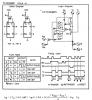
Yes a little complicated as to how the device works, but not that bad...although to be fair, I took Boolean Algebra and Symbolic Logic back in college a million years ago, both Philosophy classes. So please post if this is clear as mud...certainly not as bad as a Critique of Pure Reason or A Treatise of Human Nature.


Two inputs A and B. A third input CD. Two outputs Q and Q-bar. A and B are input either 0V (=zero) or 5V (equals 1) and, depending on the values, it will output a zero (0V) or a one (5V) on pin Q and the opposite on Q-bar. Well, actually, it does not look at the state (voltage) on the pins but rather looks for a transition from low to high or high to low. CD is a way to stop the chip from doing anything, basically a chip on-off switch, high (5V) is on, low (0V) is off. And btw, Q and Q-bar do not stay that way after a transition on A or B. They transit, then return to there original state (voltage) after a certain time. They pulse.
The time (width) of the pulse is set using this formula and the value of the resistor and capacitor:
Pulse width = (0.2+0.1[(5-0)/5])RC = 0.3RC
This is the equation that determines the pulse width. The supply voltage (Vdd) is 5V and the other side is ground (Vss). I had to trace that out on the PCB to #19 and #20 interconnect since it is not really shown anywhere else in the service manual.
Yes a little complicated as to how the device works, but not that bad...although to be fair, I took Boolean Algebra and Symbolic Logic back in college a million years ago, both Philosophy classes. So please post if this is clear as mud...certainly not as bad as a Critique of Pure Reason or A Treatise of Human Nature.
Two inputs A and B. A third input CD. Two outputs Q and Q-bar. A and B are input either 0V (=zero) or 5V (equals 1) and, depending on the values, it will output a zero (0V) or a one (5V) on pin Q and the opposite on Q-bar. Well, actually, it does not look at the state (voltage) on the pins but rather looks for a transition from low to high or high to low. CD is a way to stop the chip from doing anything, basically a chip on-off switch, high (5V) is on, low (0V) is off. And btw, Q and Q-bar do not stay that way after a transition on A or B. They transit, then return to there original state (voltage) after a certain time. They pulse.
The time (width) of the pulse is set using this formula and the value of the resistor and capacitor:
Pulse width = (0.2+0.1[(5-0)/5])RC = 0.3RC
This is the equation that determines the pulse width. The supply voltage (Vdd) is 5V and the other side is ground (Vss). I had to trace that out on the PCB to #19 and #20 interconnect since it is not really shown anywhere else in the service manual.
Last edited:
mootej
Active Member
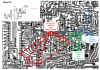
Signal E2

The way this circuit should work, a transition from low to high (leading edge) of signal E2 at pin 4 of IC10a results in a pulse from high to low at pin 7 of IC10a. The pulse lasts from 0.003 to 0.144 seconds depending on how much resistance is set on the potentiometer on S-0055, the delay adjust potentiometer VR1. At the end of the time interval, the pulse transitions back from low to high, triggering IC10b at pin 12. This is essentially a mechanism to delay the signal.
Triggering IC10b pin 12 results in the creation of a low to high transition at pin 10 for 0.09588 seconds, then a return transition from high to low when the time interval expires. The pulse is input to the microprocessor pin 2 of uPD-546-150, the PC0 input of the MPU.
A side note, uPD-546-150 is a special hard-programmed (mask ROM) microprocessor from the NEC uCOM-43 series of 4-bit processors.
Summary, signal E2 comes from Stage 3 of the op-amps as an off-on signal between 0 and 5V when the E-sensor (leading sensor) transitions from a groove to a gap in the vinyl. This triggers an adjustable delay and then produces a pulse that is input to the MPU. Here’s the service manual description of what signal E2 does…

BTW, I think the delay circuit is a really cool piece of work! Very neat way to do this.
Back to the bench to make some measurements...
The way this circuit should work, a transition from low to high (leading edge) of signal E2 at pin 4 of IC10a results in a pulse from high to low at pin 7 of IC10a. The pulse lasts from 0.003 to 0.144 seconds depending on how much resistance is set on the potentiometer on S-0055, the delay adjust potentiometer VR1. At the end of the time interval, the pulse transitions back from low to high, triggering IC10b at pin 12. This is essentially a mechanism to delay the signal.
Triggering IC10b pin 12 results in the creation of a low to high transition at pin 10 for 0.09588 seconds, then a return transition from high to low when the time interval expires. The pulse is input to the microprocessor pin 2 of uPD-546-150, the PC0 input of the MPU.
A side note, uPD-546-150 is a special hard-programmed (mask ROM) microprocessor from the NEC uCOM-43 series of 4-bit processors.
Summary, signal E2 comes from Stage 3 of the op-amps as an off-on signal between 0 and 5V when the E-sensor (leading sensor) transitions from a groove to a gap in the vinyl. This triggers an adjustable delay and then produces a pulse that is input to the MPU. Here’s the service manual description of what signal E2 does…
BTW, I think the delay circuit is a really cool piece of work! Very neat way to do this.
Back to the bench to make some measurements...
mootej
Active Member
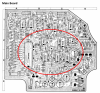
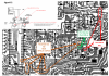
First one E2a in on channel 1 and E2a out on the first multistable multivibrator...
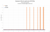
Well, now, that's interesting, 4.6V Signal E Stage 3 coming in but nothing coming out.
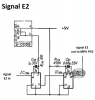
Voltmeter:
pins 8 (Vss) to pin 16 (Vdd) measures +5v -> supply is good, chip is getting power
pin 3, 5, 11,13 all at +5V -> good, pins tied high
pin2 to pin1 is in the mV range for IC10a, 2 appears to be maybe 100mV negative (!) with respect to pin 1 -> this is not right!
All of the other TC4528P chips pin2 / pin14 appear to be +5V with respect to pin1 / pin15.
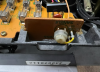
So something is wrong with IC10a timing circuit. There are three components, the tantalum cap, a resistor and a potentiometer on the S-0055 circuit board (the delay adjust). There it is! Pin4 on S-0055 is reading +5V but pin5, nothing. The potentiometer VR1on S-0055 is measuring at 3M-ohm (should be 470K-ohm) and adjusting it does not change the resistance.
Looks like a bad pot. Unfortunately, they will not have this at the local dispensary, so I may need to order one.
Anyway, this is looking up! Finally found something wrong. In the meantime, I'll see if I can check the other signals.
Here's the offending pot:
Well, now, that's interesting, 4.6V Signal E Stage 3 coming in but nothing coming out.
Voltmeter:
pins 8 (Vss) to pin 16 (Vdd) measures +5v -> supply is good, chip is getting power
pin 3, 5, 11,13 all at +5V -> good, pins tied high
pin2 to pin1 is in the mV range for IC10a, 2 appears to be maybe 100mV negative (!) with respect to pin 1 -> this is not right!
All of the other TC4528P chips pin2 / pin14 appear to be +5V with respect to pin1 / pin15.
So something is wrong with IC10a timing circuit. There are three components, the tantalum cap, a resistor and a potentiometer on the S-0055 circuit board (the delay adjust). There it is! Pin4 on S-0055 is reading +5V but pin5, nothing. The potentiometer VR1on S-0055 is measuring at 3M-ohm (should be 470K-ohm) and adjusting it does not change the resistance.
Looks like a bad pot. Unfortunately, they will not have this at the local dispensary, so I may need to order one.
Anyway, this is looking up! Finally found something wrong. In the meantime, I'll see if I can check the other signals.
Here's the offending pot:
Last edited:
mootej
Active Member
I'll admit, I like replacing failed stuff with original if possible. I should probably go the other route and replace with better than original and new, but I couldn't resist. This is from an FR-D55 and VR4 is the correct donor part, the exact 470K trim pot. OK, I overpaid for an old, untested trim pot but it "looks" the same as the original. Nobody will ever know...

It is interesting, when the Sansui engineers redesigned the FR-D55 from the XR-Q11, they moved all of the adjustment trim pots to a separate circuit board and accessible from the top without removing the cabinet or bottom panel. Great guys those Sansui engineers!

It turns out this is the exact same trim pot with the exact same purpose as for the XR-Q11. And, while noodling around searching Sansui parts on Ebay, I was also able to pick up a dustcover with hinges for the FR-D55! Turns out the same dustcover was used for a bunch of Sansui models. Can't wait to tackle the FR-D55, it will be a piece of cake now that I know how this works and what the signals should look like...
It is interesting, when the Sansui engineers redesigned the FR-D55 from the XR-Q11, they moved all of the adjustment trim pots to a separate circuit board and accessible from the top without removing the cabinet or bottom panel. Great guys those Sansui engineers!
It turns out this is the exact same trim pot with the exact same purpose as for the XR-Q11. And, while noodling around searching Sansui parts on Ebay, I was also able to pick up a dustcover with hinges for the FR-D55! Turns out the same dustcover was used for a bunch of Sansui models. Can't wait to tackle the FR-D55, it will be a piece of cake now that I know how this works and what the signals should look like...