After seeing the readings above, I decided to land the lifted leg of R701. I energized it briefly, and within 2 secs, the protection relay closed. I did have the speaker 1 switch selected to ON. I then down powered it. I wanted to hear from you before I started trying to set main amp voltages (L & R).


You are using an out of date browser. It may not display this or other websites correctly.
You should upgrade or use an alternative browser.
You should upgrade or use an alternative browser.
2252B power/amp brd issues
- Thread starter mgl99
- Start date
-
- Tags
- 2252b power supply issues

With it on, do a quick check on those -36v around Q701 and Q703, then check voltage around Q715 and Q717. You want to make sure that the emitters to Q715 & Q717 are close to 0v, not 36V. If all looks good, I think you can try to set adjust voltages. Are Q711 and Q713 installed now? Make sure that the transistors are installed in the correct positions. Post any voltages you measure and we can review.
Last edited:
Well, a little step backward. I installed Q711 and Q713 in their correct locations. I looked everything over, and then energized it. The PR closed in and I didn't see any immediate over heating problems.
I quickly measured J122 to chassis Gnd: 35.14 VDC. I then quickly measured Q701 (e) to chassis Gnd: 0.757 VDC and Q703 (e) to chassis Gnd 0.687 VDC. I then measured Q715 (e) and Q717 (e) . The readings to Gnd were both around 0.6 VDC.
At that moment, I noticed a whiff of smoke. I immediately down powered. Damage as follows: R721 Overheated, R728 Badly overheated, and resistance readings on Q705 (e) to (b) 31.7 ohms, and Q706 (e) to (b) 1.040 K ohms, indicating to me, that once again Q705 has failed along with R721 which had previously failed and been replaced, as was Q705 and Q706 (for consistency).
I visually inspected the back of the board in the vicinity of the failed components. No damage, but how many other components have now failed?
I quickly measured J122 to chassis Gnd: 35.14 VDC. I then quickly measured Q701 (e) to chassis Gnd: 0.757 VDC and Q703 (e) to chassis Gnd 0.687 VDC. I then measured Q715 (e) and Q717 (e) . The readings to Gnd were both around 0.6 VDC.
At that moment, I noticed a whiff of smoke. I immediately down powered. Damage as follows: R721 Overheated, R728 Badly overheated, and resistance readings on Q705 (e) to (b) 31.7 ohms, and Q706 (e) to (b) 1.040 K ohms, indicating to me, that once again Q705 has failed along with R721 which had previously failed and been replaced, as was Q705 and Q706 (for consistency).
I visually inspected the back of the board in the vicinity of the failed components. No damage, but how many other components have now failed?
It appears that there is something else wrong with either your board or one component. I had asked before, but can you post a 'good', readable photo of the front and backside of the board so I can compare it with mine. Shine a lamp on the board or in sun light so I can read the parts. Clearly show where you soldered the backside components onto the traces. From the schematic the component that is common to both sections is C729 220uF/50v. Make sure that the (+) side is to Gnd. Thanks.
EDIT:
You did put the power transistors in this way... right (with the two PNPs towards the middle, and NPNs towards the ends)?
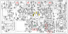
EDIT:
You did put the power transistors in this way... right (with the two PNPs towards the middle, and NPNs towards the ends)?
Last edited:
Aha, I think I found it... staring us in the face all along. Unless a component has changed from Wayyyy back in the beginning, C721 (yellow arrow) is installed backward! See board photo vs board layout. Best to put in a new one.
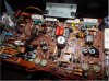
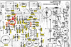
Here on the board layout diagram (highlighted all bad channel components in yellow).
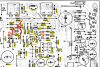
Here on the board layout diagram (highlighted all bad channel components in yellow).
Last edited:
I read your last post. I will go out and check the orientation of C721 as installed. I want to understand exactly what you are saying about C729. Your statement was " From the schematic the component that is common to both sections is C729 220uF/50v. Make sure that the (+) side is to Gnd." Are you saying that the silkscreen board markings are wrong for C729 polarity??
I will definitely look into these issues right away. Here is what I have done today. I replaced R721, R728, and Q705. Q705 was shorted from (e) to (b) as tested by the DCA55 after removal. I checked Q706 in situ, and it showed normal resistance readings.
After replacing R721, I did point to point checks to make sure the traces were okay. I discovered that the trace between R721 and Q705 (e) was reading OPEN. I don't know when this occurred. I jumpered the damaged trace section and tested all close and connecting points to verify continuity, and that no unwanted shorts existed.
I was hoping that we might come up with a plan of resistance readings before energizing again. I'm headed out to check C721 and C729. Back soon.
I will definitely look into these issues right away. Here is what I have done today. I replaced R721, R728, and Q705. Q705 was shorted from (e) to (b) as tested by the DCA55 after removal. I checked Q706 in situ, and it showed normal resistance readings.
After replacing R721, I did point to point checks to make sure the traces were okay. I discovered that the trace between R721 and Q705 (e) was reading OPEN. I don't know when this occurred. I jumpered the damaged trace section and tested all close and connecting points to verify continuity, and that no unwanted shorts existed.
I was hoping that we might come up with a plan of resistance readings before energizing again. I'm headed out to check C721 and C729. Back soon.
No, what I'm saying is to check the polarity of that cap as, in the past and now, you have made errors in installing some of the new caps.Make sure that the (+) side is to Gnd." Are you saying that the silkscreen board markings are wrong for C729 polarity??
Last edited:
This is my report on C721 and C729. C721 is installed correctly from what I found. First off, it is in per the silkscreen markings on the board. Secondly, I tested continuity with my DMM between the (+) side of C721 and (-) side of C719. It reads 0.0 ohms. I then checked continuity between the (-)side of C721 to R741 (one side). It read 0.0 ohms. I read from the (+) side of C729 to J703. It read 0.0 ohms.
All of these readings agree with the schematic. I would appreciate you explaining why you think C721 and C729 are in wrong, because I'm not seeing that. I also visually checked the remaining electrolytic caps on the board, and they are installed per the polarity markings on the board. The only exception, is C701, since it is known that the markings on the board are incorrect. That issue was corrected earlier.
Please help me understand the problem with C721 and C729.
I took ten pics this morning of the top and bottom of the board, and they all came out blurry. I'm going to get my camera tripod and get some clearer pics after lunch. I wanted to post the data on C721 and C729 first.
All of these readings agree with the schematic. I would appreciate you explaining why you think C721 and C729 are in wrong, because I'm not seeing that. I also visually checked the remaining electrolytic caps on the board, and they are installed per the polarity markings on the board. The only exception, is C701, since it is known that the markings on the board are incorrect. That issue was corrected earlier.
Please help me understand the problem with C721 and C729.
I took ten pics this morning of the top and bottom of the board, and they all came out blurry. I'm going to get my camera tripod and get some clearer pics after lunch. I wanted to post the data on C721 and C729 first.
EDIT: I'm looking at photos of my 2252B when I recapped it and C721 looks to be in the same orientation as yours, but in the SM the '+' sign is shown as the opposite on the board layout. I need to review this... so disregard the following explanation until I investigate.
**** Nevermind - found another error in the SM, board layout. It shows C721 cap '+' incorrectly oriented. ****
See my board below -- matches your photo for C721.

C729 looks OK, thanks.
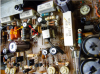
Now look at the SM board layout for C721 (red arrow) below. The silkscreen shows the (+) side of C721 toward the Right and (-) to the Left.
Compare this to the C721 installed on your board above. You can clearly see that your installed cap (photo) has the (-) to the right vs. this board layout with (-) to the left!
**** Nevermind - found another error in the SM, board layout. It shows C721 cap '+' incorrectly oriented. ****
See my board below -- matches your photo for C721.
C729 looks OK, thanks.
C721 is installed correctly from what I found.
Your C721 is installed backward with the (-) side where the (+) should be!I would appreciate you explaining why you think C721 and C729 are in wrong, because I'm not seeing that.
Here is a photo of your board with yellow arrow pointing to C721 and red arrow pointing to the (-) side as YOU have it installed.Please help me understand the problem with C721 and C729.
Now look at the SM board layout for C721 (red arrow) below. The silkscreen shows the (+) side of C721 toward the Right and (-) to the Left.
Compare this to the C721 installed on your board above. You can clearly see that your installed cap (photo) has the (-) to the right vs. this board layout with (-) to the left!
Last edited:
I'm sorry, I just got back 20 mins. ago. I went back out and looked at everything again. There is a (+) sign visible for C721. I want to make sure, I am right, so I'm going to pull C721, and now that I've got the tripod at the workbench, I will take a picture of it. IF it is in backward, then why did all of the readings I took and showed you, came out right in accordance with the schematic. I didn't go by the layout drawing, I go by the the schematic. If the cap were in backwards, all of those readings should have been bad.
Also, I was wondering if you looked at your board in your unit, to see how they are installed. If C721 is in backward, then so must C722 be in backwards. Anyway, I'll unsolder C721 and get pics. I do agree with you that the location drawing casts doubt, but what about the continuity readings?
Also, I was wondering if you looked at your board in your unit, to see how they are installed. If C721 is in backward, then so must C722 be in backwards. Anyway, I'll unsolder C721 and get pics. I do agree with you that the location drawing casts doubt, but what about the continuity readings?
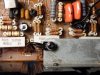
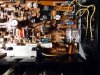
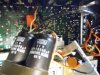
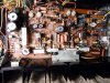
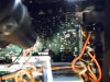
I certainly hope you are still on board. Last time I energized it, I lost R721, R728, and Q705. I'm trying to figure that out also. It may have been that Q705 was bad at the time I energized. I don't know if that alone could have caused the resistors to overheat. All have been replaced now. What would you recommend at this point? Power up briefly to take live readings, or to stay down and take some resistance readings?
I do have the output transistors in the correct place. They match with your drawing, my before photos, and a drawing I made before pulling them. They all still test good on the DCA55.
I do have the output transistors in the correct place. They match with your drawing, my before photos, and a drawing I made before pulling them. They all still test good on the DCA55.
Thanks for the photos. I noticed something for you to check.
Take a look at varistor Q741 mounted on the heatsink on your unit.
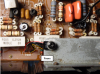
Compare it to my 2252B. If the date code stamped on the part (or the orange dot on the side) indicate the polarity of the diode, then they are installed differently.
From what I found online, the cathode seems to be the wire on the "yellow dot" on the side of the part. I can't tell from the photo what side is yours.
I have never removed mine, have you removed or replaced yours?
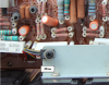
Here, I tried to trace through the path of destruction to see where the high current to burn out two resistors and 1 transistor came from.
Look at the violet colored dotted lines and arrows. It goes from where the (-) voltage comes into the board, goes throught the two resistors R728, R721, and to Q705.
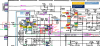
Where does the high current come from?
1. Probably not the base of Q705 since it is at about the same (-) voltage
2. From Q709 (b), should be -1.1 but was measured before at 38v
3. The Q709 (c) is connected to Q741 varistor (follow purple arrows). We know before it had a voltage of 38V on both anode and cathode.
4. We know from the measurement on the other side, Q742 that you previously measured +1.3V (A), -1.3V (C).
5. The last thing that we can think of is to compare resistance measurements to ground again for Q705 and surrounding components in this purple path and compare with Q706, the good channel.
Found this older photo of yours (disregard my other markings). I don't see the dot on this side so maybe your date code is stamped on the opposite side of the part.

It's a long shot, but I don't know where to look next.
Take a look at varistor Q741 mounted on the heatsink on your unit.
Compare it to my 2252B. If the date code stamped on the part (or the orange dot on the side) indicate the polarity of the diode, then they are installed differently.
From what I found online, the cathode seems to be the wire on the "yellow dot" on the side of the part. I can't tell from the photo what side is yours.
I have never removed mine, have you removed or replaced yours?
Here, I tried to trace through the path of destruction to see where the high current to burn out two resistors and 1 transistor came from.
Look at the violet colored dotted lines and arrows. It goes from where the (-) voltage comes into the board, goes throught the two resistors R728, R721, and to Q705.
Where does the high current come from?
1. Probably not the base of Q705 since it is at about the same (-) voltage
2. From Q709 (b), should be -1.1 but was measured before at 38v
3. The Q709 (c) is connected to Q741 varistor (follow purple arrows). We know before it had a voltage of 38V on both anode and cathode.
4. We know from the measurement on the other side, Q742 that you previously measured +1.3V (A), -1.3V (C).
5. The last thing that we can think of is to compare resistance measurements to ground again for Q705 and surrounding components in this purple path and compare with Q706, the good channel.
Found this older photo of yours (disregard my other markings). I don't see the dot on this side so maybe your date code is stamped on the opposite side of the part.
It's a long shot, but I don't know where to look next.
Last edited:

If you're still going to work on it, don't power up until you do the "diode test" to every semiconductor in the bad channel. I don't recommend removal and DCA test for that, more damage / shorts could be created. Honestly, it's time to get it to a seasoned tech.
I did notice that my "diode" has the number 84B on it, and yours has the number 82C on it. I'll look again, but I didn't see any yellow dots on mine. Isn't there a test I could do on it? I'll check everything again, but what I was thinking was that if there were a place I could monitor voltage, I could do quick powered readings, but only have it on long enough to get a reading. This morning I measured resistance between the three legs of Q705 (not to chassis Gnd) to each other. They do pretty much mimic what I see on Q706.
Well, I made the decision to get some powered readings. I'll start with a few, and then see if they lead me in a direction.
I used mini-grabbers and obtained the following readings to Chassis Gnd:
Q709
E 38.43 VDC
C -39.19 VDC
B 38.43 VDC
This is what I've got for now, but it's a far and away from -1.1 VDC !
I tried to test the diodes in situ, however they are both jumpered with 470 ohm 1/4W resistors (back side). Even the ESR tester I have, isn't going to test a resistor in parallel with a diode; at least with any dependability or accuracy. I did take a lot of resistance readings on Q705 and Q706 (in situ). The readings were substantially the same.
Back to the schematic.
I used mini-grabbers and obtained the following readings to Chassis Gnd:
Q709
E 38.43 VDC
C -39.19 VDC
B 38.43 VDC
This is what I've got for now, but it's a far and away from -1.1 VDC !
I tried to test the diodes in situ, however they are both jumpered with 470 ohm 1/4W resistors (back side). Even the ESR tester I have, isn't going to test a resistor in parallel with a diode; at least with any dependability or accuracy. I did take a lot of resistance readings on Q705 and Q706 (in situ). The readings were substantially the same.
Back to the schematic.
Last edited:
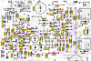
Opened up my 2252B and took some resistance readings of the resistors with power off, main caps discharged, and by discharging each resistor lead before reading ohms to chassis ground.
Here is what I got. See if you can compare it to yours and if there is a major difference somewhere that may lead to a clue.
Is Q715 original, or did you replace it? If you replaced it, what with?
Here is what I got. See if you can compare it to yours and if there is a major difference somewhere that may lead to a clue.
Is Q715 original, or did you replace it? If you replaced it, what with?
Last edited:
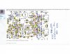
Here are readings that I have taken so far. I hope you can read my chicken scratch. I discharged the filter caps and every resistor, before I tested to chassis Gnd for the reading. Regardless, the readings took quite awhile to stabilize, because there are still caps in line. It appears that my readings are quite different from yours so far. I will continue taking readings on the other resistors to Gnd. As far as Q715 is concerned, I did not replace it. It is the original. I will post readings as I get them. I think this is a very good idea. I took readings on R762 and R764 to compare to.
Last edited: