

You are using an out of date browser. It may not display this or other websites correctly.
You should upgrade or use an alternative browser.
You should upgrade or use an alternative browser.
b&k st-120 power amplifier
- Thread starter groucho69
- Start date
-
- Tags
- b&k channel a no sound st-120


JoseHH
Super Member
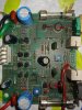
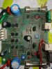
The gate drivers are the ones that you marked with the fat arrow. The other two I am not sure what is their role because I have no schematic.
If they are ok. Test the red led.
The red LED and one of the transistors that you just measured form a current source. That current passes through a network of resistors and generates the idle gate voltages. The blue variable resistor closest to the arrows you marked is in the resistor network that I mentioned. Do not change the setting of the variable resistor until we know what is faulty.
When you remove transistors, you can also check resistor values around that zone of the circuit to see if there is an open resistor. To test resistors, you can lift one of the resistor leads, measure write down the resistor and the screen print on the board to identify it. Also, those transistors that you are measuring are identified with a screen print on the board. Q1, etc. So far none of the components that you tested are bad.
If they are ok. Test the red led.
The red LED and one of the transistors that you just measured form a current source. That current passes through a network of resistors and generates the idle gate voltages. The blue variable resistor closest to the arrows you marked is in the resistor network that I mentioned. Do not change the setting of the variable resistor until we know what is faulty.
When you remove transistors, you can also check resistor values around that zone of the circuit to see if there is an open resistor. To test resistors, you can lift one of the resistor leads, measure write down the resistor and the screen print on the board to identify it. Also, those transistors that you are measuring are identified with a screen print on the board. Q1, etc. So far none of the components that you tested are bad.
Last edited:

groucho69
Member
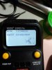
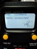
The gate drivers are the ones that you marked with the fat arrow. The other two I am not sure what is their role because I have no schematic. these are the 2N5210.
If they are ok. Test the red led.
The red and one of the transistors that you just measured form a current source. That current passes through a network of resistors and generates the idle gate voltages. The blue variable resistor closest to the arrows you marked is in the resistor network that I mentioned. Do not change the setting of the variable resistor until we know what is faulty.
When you remove transistors, you can also check resistor values around that zone of the circuit to see if there is an open resistor. To test resistors, you can lift one of the resistor leads, measure write down the resistor and the screen print on the board to identify it. Also, those transistors that you are measuring are identified with a screen print on the board. Q1, etc. So far none of the components that you tested are bad.
JoseHH
Super Member
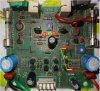
Please measure the values of the resistances Ra and Rb I marked in the following picture:
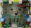
Rb is to know what is the idle current setting
Ra is to know what is the DC offset setting
I could not find any schematic for this ST-120 amplifier. So I made a schematic diagram by following the tracks of the printed circuit and component pictures that you uploaded, and the diagrams from other BK models:
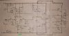
The positive rail is on top, the negative rail is on the bottom. The yellow line is the negative feedback. Note that there are 3 points grounded at the RCA input connector (RCA_GND) and a separate ground wire that goes to the power supply star GND (labeled PS_GND). Some resistor values are unknown to me at this moment since I do not have this amplifier with me to measure them. I will complete that later.
I am not 100% sure if this diagram is mistake free. If somebody in this forum finds a mistake (or if a better schematic) I will appreciate any comment with corrections.
Rb is to know what is the idle current setting
Ra is to know what is the DC offset setting
I could not find any schematic for this ST-120 amplifier. So I made a schematic diagram by following the tracks of the printed circuit and component pictures that you uploaded, and the diagrams from other BK models:
The positive rail is on top, the negative rail is on the bottom. The yellow line is the negative feedback. Note that there are 3 points grounded at the RCA input connector (RCA_GND) and a separate ground wire that goes to the power supply star GND (labeled PS_GND). Some resistor values are unknown to me at this moment since I do not have this amplifier with me to measure them. I will complete that later.
I am not 100% sure if this diagram is mistake free. If somebody in this forum finds a mistake (or if a better schematic) I will appreciate any comment with corrections.
Last edited:
JoseHH
Super Member
I am sorry. I think i did not explain myself very well.
I meant the resistance values between pairs of arrows. If you touch with your DVM between the points I marked with the arrows you get the readings for the variable resistors. I want to take note of what those resistances are. For Ra you measure the resistance between the pair of arrows near the label Ra (the two arrows I connected with a yellow line) , and similarly for Rb, which is a lead of a diode and a lead of a resistor, which are convenient points to measure from the top side.
I meant the resistance values between pairs of arrows. If you touch with your DVM between the points I marked with the arrows you get the readings for the variable resistors. I want to take note of what those resistances are. For Ra you measure the resistance between the pair of arrows near the label Ra (the two arrows I connected with a yellow line) , and similarly for Rb, which is a lead of a diode and a lead of a resistor, which are convenient points to measure from the top side.
JoseHH
Super Member
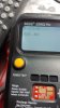
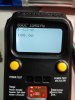
So far all the components that you tested are ok. You said the both fuses on the board tested ok?. There is a resistor under each fuse. Please measure those also. I want to complete the schematic. If you are careful, you can test each transistor, write down the part number, hfe and Vbe, and identification (Q1, Q2, etc). If all the transistors are ok, then test the zener diode (the grey diode near the input of the board), and please try to see with a magnifying glass or by taking a photo with a mobile phone in "macro setting" so we can know what sort of zener it is. I know that all the other diodes are 1N4148, so no need to photograph those.
If you look at the schematic, you will see that this model has some protection circuit (which I put on the right side of the diagram) this portion of the circuit will pull down the gate voltage in case of excessive current. So if one of the transistors (2N5551 or 2N5401) becomes shorted, you will get no output. So, please check those transistors also.
If you look at the schematic, you will see that this model has some protection circuit (which I put on the right side of the diagram) this portion of the circuit will pull down the gate voltage in case of excessive current. So if one of the transistors (2N5551 or 2N5401) becomes shorted, you will get no output. So, please check those transistors also.
JoseHH
Super Member
So what where the readings for Ra and Rb?
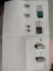
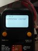
Also, if you have the chance, please inspect this zener diode (circled in yellow in the next image) and try to see if you can read the part number on it. You may have to remove it from the board to do this. I am not sure if your tester can test this zener, but please give it a try if you take it out.
Dont forget to test the red LED also.
Also, if you have the chance, please inspect this zener diode (circled in yellow in the next image) and try to see if you can read the part number on it. You may have to remove it from the board to do this. I am not sure if your tester can test this zener, but please give it a try if you take it out.
Dont forget to test the red LED also.
Attachments

Similar threads

- Replies
- 2
- Views
- 858


- Replies
- 7
- Views
- 6K
