• The move to the new server is done. There are some software and database maintenance updates in process. This has us passing the hat around to help out. We appreciate any donations. Seriously, even a dollar helps. The payment page may be found here - https://www.audiokarma.org/support.html

Repair Pioneer A9 NSA

the paralleling of two 150 ohm 1/2 w resistors to make 75 ohms with 1 watt dissipation is perfectly fine.

The mismatch of those failure points is dwarfed by the capabilities of a serious fault. They'll pop just fine...
The objective IS to have NO faults.
Thank you for the quick response ,Markthefixer - we saved one delivery and waiting until Tuesday. Just in time before I order them! I have them and now I will solder them and write when done
 
the paralleling of two 150 ohm 1/2 w resistors to make 75 ohms with 1 watt dissipation is perfectly fine.

The mismatch of those failure points is dwarfed by the capabilities of a serious fault. They'll pop just fine...
The objective IS to have NO faults.
I made the resistор of 75 Ohm 1W from two parallel 150 Ohm 1/2 Watt, I replaced R1 of GWX-593 L channel with it. I soldered the middle point of this resistор to pin number 5, where the white cable goes to the + L on output. I checked the resistance pin 5 to the emitter of Q1 is 75 Ohm and pin 5 to the emitter of Q3 is 75.1 Ohm. The same goes for the WX-594 right driver board. I connected the midpoint of the resistor R2 2x75 Ohms 1Watt to pin 10 where the +R output gray cable comes out. I measured the resistance between pin 10 and the emitter of Q2 is 75 ohms and pin 10 to the emitter of Q4 is also 75 ohms. Now I am ready to connect the boards and all the connectors and circuits and measure the voltages of all the transistors from the driver boards as I measured and posted them in #23. I will await approval or new instructions.
 
post #47 resistor changes approved.

since you like to use a dash as a separator, could i ask that you use the + symbol for positive voltages?
 
20220708_213044.jpg
post #47 resistor changes approved.

since you like to use a dash as a separator, could i ask that you use the + symbol for positive voltages?

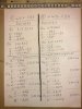
This was a long measurement. I measured the data several times because it turned out that it varies with time and temperature of the elements. For this reason I have written in some places 2 values from min to max and between them two dots with a dash. I also re soldered a fuming solder on the power supply board to one of the small Grez rectifier diodes This did not affect performance and measurements.

First, I connected the amplifier through the DBT and after seeing that there was no short, I turned it on at 120V. After a few seconds, the protection turned off and the green light came on. I immediately measured the voltage at the speaker outputs.

On the +terminals L and R right after switching on it is 0.011v, which after 5 min. becomes 0.004v for both channels. On the negative terminal is 0v .All 4 VRs on the amplifier board are turn at full counter clock ways.
I post the data in the photo. At the end of each measurement after about 20 minutes the heat sink of the driver transistors was very hot. With the exception of Q1, the rest of the heat sinks cannot be held by hand for more than 2 seconds. Q1 heat sync can be held by hand for a long time and it is warm but it is normal. This is the data. I can provide any other measurements needed or replace items as per the following instructions.
Correction made .
 
Last edited:
The measurements now need to be made at the "output" of the NSA circuits.

Q25 & Q27 are a pair of current source/sinks that supply a current centered on the instantaneous output voltage of the amp.
This current is turned into a control voltage for the NSA circuits.
by current flowing through :
R101, D11, D13, D15, D17, R103
and the center is between D13 & D15.
the voltage at R101 is fed to Q19 & Q17, the nsa circuit for the positive portion of the push pull circuit.
the voltage at R103 is fed to Q23 & Q21, the nsa circuit for the negative portion of the push pull circuit.
Q17 & Q21 are coupled by the VR1 0 to 100 ohm pot and the stv-4h diode.
This all develops a positive and negative voltage (centered around the output voltage) that drives the predrivers, drivers and output transistors.
Each step (predriver to driver, driver to output, output to emitter resistors)loses 0.6v to the Vbe drop at that stage.
This voltage is controlled by the VR1, 100 ohm pot.

What I would expect to see (at specified 75 mA idle current, assuming perfect 0.600v vbe transistors) is
+1.837 Q29 (predriver) base,
+1.237 Q29 (predriver) emitter, (move to GWX-593) Q1 (driver) base,
+0.637 Q1 (driver) emitter, Q1(o/p) & Q3(o/p) base,
+0.037 Q1(o/p) & Q3(o/p) emitter (*** idle current!! )
-0.037 Q2(o/p) & Q4(o/p) emitter (*** idle current!! )
-0.637 Q3 (driver) emitter, Q2(o/p) & Q4(o/p) base,
-1.237 Q31 (predriver) emitter, (move to GWX-593) Q3 (driver) base,
-1.837 Q31 (predriver) base

But nothing's perfect, my experience is based on nsa circuits that use STV-2H diodes, NOT STV-4H diodes. There will probably be more voltage, but I'm just trying to illuminate some theory here.

do we have that VR1 control? This will tell.

BUNCH of voltage reading requests below.

Confirm VR1 ( 0 to 100 ohms) is zero ohms
GWH-146 Q29 & Q31 bases. (predriver)
GWH-146 Q29 & Q31 emitters. (predriver)
GWX-593 Q1 base & Q3 base (drivers)
GWX-593 Q1 emitter & Q3 emitter (drivers)

(no outputs, so we stop at the driver stage, who's output is around 0.600 volts)

Increase VR1 ( 0 to 100 ohms) to 25 ohms
GWH-146 Q29 & Q31 base.
GWH-146 Q29 & Q31 emitter.
GWX-593 Q1 base & Q3 base
GWX-593 Q1 emitter & Q3 emitter

Increase VR1 ( 0 to 100 ohms) to 50 ohms
GWH-146 Q29 & Q31 base.
GWH-146 Q29 & Q31 emitter.
GWX-593 Q1 base & Q3 base
GWX-593 Q1 emitter & Q3 emitter

Increase VR1 ( 0 to 100 ohms) to 75 ohms
GWH-146 Q29 & Q31 base.
GWH-146 Q29 & Q31 emitter.
GWX-593 Q1 base & Q3 base
GWX-593 Q1 emitter & Q3 emitter

Decrease VR1 to zero ohms.

now for the other channel

Confirm VR2 ( 0 to 100 ohms) is zero ohms
GWH-146 Q30 & Q32 base.
GWH-146 Q30 & Q32 emitter.
GWX-594 Q2 base & Q4 base
GWX-594 Q2 emitter & Q4 emitter

Increase VR2 ( 0 to 100 ohms) to 25 ohms
GWH-146 Q30 & Q32 base.
GWH-146 Q30 & Q32 emitter.
GWX-594 Q2 base & Q4 base
GWX-594 Q2 emitter & Q4 emitter

Increase VR2 ( 0 to 100 ohms) to 50 ohms
GWH-146 Q30 & Q32 base.
GWH-146 Q30 & Q32 emitter.
GWX-594 Q2 base & Q4 base
GWX-594 Q2 emitter & Q4 emitter

Increase VR2 ( 0 to 100 ohms) to 75 ohms
GWH-146 Q30 & Q32 base.
GWH-146 Q30 & Q32 emitter.
GWX-594 Q2 base & Q4 base
GWX-594 Q2 emitter & Q4 emitter

Decrease VR2 to zero ohms.

These investigate the first part of the NSA circuits. the VR1 part that is initially set at 50 millivolts.
later we'll get the second part, the 75 millivolt setpoint.

Be advised, when output transistors are connected, there will be no apparent reaction as VR1(&VR2) is turned up, UNTIL it overcomes all Vbe drops and actual current begins to flow in the output transistors. THEN it will take effect very very quickly, so if the VR1 real live adjustment is done too quickly the target idle current could EASILY be overshot with that setting dangerously high.

This ALSO occurs with the VR3 & VR4 adjustments - they suddenly "come live" and are very sensitive.
 
Last edited:
The measurements now need to be made at the "output" of the NSA circuits.

Q25 & Q27 are a pair of current source/sinks that supply a current centered on the instantaneous output voltage of the amp.
This current is turned into a control voltage for the NSA circuits.
by current flowing through :
R101, D11, D13, D15, D17, R103
and the center is between D13 & D15.
the voltage at R101 is fed to Q19 & Q17, the nsa circuit for the positive portion of the push pull circuit.
the voltage at R103 is fed to Q23 & Q21, the nsa circuit for the negative portion of the push pull circuit.
Q17 & Q21 are coupled by the VR1 0 to 100 ohm pot and the stv-4h diode.
This all develops a positive and negative voltage (centered around the output voltage) that drives the predrivers, drivers and output transistors.
Each step (predriver to driver, driver to output, output to emitter resistors)loses 0.6v to the Vbe drop at that stage.
This voltage is controlled by the VR1, 100 ohm pot.

What I would expect to see (at specified 75 mA idle current, assuming perfect 0.600v vbe transistors) is
+1.837 Q29 (predriver) base,
+1.237 Q29 (predriver) emitter, (move to GWX-593) Q1 (driver) base,
+0.637 Q1 (driver) emitter, Q1(o/p) & Q3(o/p) base,
+0.037 Q1(o/p) & Q3(o/p) emitter (*** idle current!! )
-0.037 Q2(o/p) & Q4(o/p) emitter (*** idle current!! )
-0.637 Q3 (driver) emitter, Q2(o/p) & Q4(o/p) base,
-1.237 Q31 (predriver) emitter, (move to GWX-593) Q3 (driver) base,
-1.837 Q31 (predriver) base

But nothing's perfect, my experience is based on nsa circuits that use STV-2H diodes, NOT STV-4H diodes. There will probably be more voltage, but I'm just trying to illuminate some theory here.

do we have that VR1 control? This will tell.

BUNCH of voltage reading requests below.

Confirm VR1 ( 0 to 100 ohms) is zero ohms
GWH-146 Q29 & Q31 bases. (predriver)
GWH-146 Q29 & Q31 emitters. (predriver)
GWX-593 Q1 base & Q3 base (drivers)
GWX-593 Q1 emitter & Q3 emitter (drivers)

(no outputs, so we stop at the driver stage, who's output is around 0.600 volts)

Increase VR1 ( 0 to 100 ohms) to 25 ohms
GWH-146 Q29 & Q31 base.
GWH-146 Q29 & Q31 emitter.
GWX-593 Q1 base & Q3 base
GWX-593 Q1 emitter & Q3 emitter

Increase VR1 ( 0 to 100 ohms) to 50 ohms
GWH-146 Q29 & Q31 base.
GWH-146 Q29 & Q31 emitter.
GWX-593 Q1 base & Q3 base
GWX-593 Q1 emitter & Q3 emitter

Increase VR1 ( 0 to 100 ohms) to 75 ohms
GWH-146 Q29 & Q31 base.
GWH-146 Q29 & Q31 emitter.
GWX-593 Q1 base & Q3 base
GWX-593 Q1 emitter & Q3 emitter

Decrease VR1 to zero ohms.

now for the other channel

Confirm VR2 ( 0 to 100 ohms) is zero ohms
GWH-146 Q30 & Q32 base.
GWH-146 Q30 & Q32 emitter.
GWX-594 Q2 base & Q4 base
GWX-594 Q2 emitter & Q4 emitter

Increase VR2 ( 0 to 100 ohms) to 25 ohms
GWH-146 Q30 & Q32 base.
GWH-146 Q30 & Q32 emitter.
GWX-594 Q2 base & Q4 base
GWX-594 Q2 emitter & Q4 emitter

Increase VR2 ( 0 to 100 ohms) to 50 ohms
GWH-146 Q30 & Q32 base.
GWH-146 Q30 & Q32 emitter.
GWX-594 Q2 base & Q4 base
GWX-594 Q2 emitter & Q4 emitter

Increase VR2 ( 0 to 100 ohms) to 75 ohms
GWH-146 Q30 & Q32 base.
GWH-146 Q30 & Q32 emitter.
GWX-594 Q2 base & Q4 base
GWX-594 Q2 emitter & Q4 emitter

Decrease VR2 to zero ohms.

These investigate the first part of the NSA circuits. the VR1 part that is initially set at 50 millivolts.
later we'll get the second part, the 75 millivolt setpoint.

Be advised, when output transistors are connected, there will be no apparent reaction as VR1(&VR2) is turned up, UNTIL it overcomes all Vbe drops and actual current begins to flow in the output transistors. THEN it will take effect very very quickly, so if the VR1 real live adjustment is done too quickly the target idle current could EASILY be overshot with that setting dangerously high.

This ALSO occurs with the VR3 & VR4 adjustments - they suddenly "come live" and are very sensitive.
То realized this procedure I have to change VR 1,2,3,4. It turned out that they are not at zero as they are closed to the end, but at different values. This must have affected the measurements as well. I will change them and take new measurements and also the new ones that fit me. The worst is VR1, which in the closed position is 80 ohms. The transistors from Q9 to Q16 on the amplifier board heat up almost like a soldering iron. These are 2sa905 and 2sc1915. KSA1220 and KSC2690 are no longer found. What do you think about replacing 2sa905 and 2sc1915 with a KSA1381 and KSC3503? I
 
What do you think about replacing 2sa905 and 2sc1915 with a KSA1381 and KSC3503? I

YES, that is what I have been recommending for a while on various NSA models.
Replace each of the 2sa905 with a KSA1381 and each of the 2sc1915 with KSC3503.
Here is a (TO-126) heat sink for them: mouser.com 532-577500B00

The transistors from Q9 to Q16 on the amplifier board heat up almost like a soldering iron. These are 2sa905 and 2sc1915

I'm taking a closer look at Q9 through Q16 inclusive.

A lot of heat is routinely expected from Q13, Q14, Q15 & Q16. This is experience from other NSA amps.
Q15 & Q16 are a 8 mA current source, and with close to 60 volts operating, so they're dissipating about 1/2 watt on each transistor.
Q13 & Q14 are the corresponding VAS stage and they also have to shed about 1/2 watt of heat apiece.

The previous differential stage of two 2sc1915's, Q9 & Q11 (or Q10 & Q12) look to be shedding 1/4 watt of heat apiece.

If they can be fit in, I would recommend heat sinks for all of them, but if fitment becomes an issue, with Q9, Q10, Q11, Q12 shedding only 1/4 watt of heat, they
wouldn't be too heavily stressed if they did not have heat sinks. (maybe we should call them heat spreaders? they spread heat out to the air)

A picture of the GWH-146 board would be informative. The GWH-146 board mounts up against the back panel, am I correct?
 
Last edited:
YES, that is what I have been recommending for a while on various NSA models.
Replace each of the 2sa905 with a KSA1381 and each of the 2sc1915 with KSC3503.
Here is a (TO-126) heat sink for them: mouser.com 532-577500B00


I'm taking a closer look at Q9 through Q16 inclusive.

A lot of heat is routinely expected from Q13, Q14, Q15 & Q16. This is experience from other NSA amps.
Q15 & Q16 are a 8 mA current source, and with close to 60 volts operating, so they're dissipating about 1/2 watt on each transistor.
Q13 & Q14 are the corresponding VAS stage and they also have to shed about 1/2 watt of heat apiece.

The previous differential stage of two 2sc1915's, Q9 & Q11 (or Q10 & Q12) look to be shedding 1/4 watt of heat apiece.

If they can be fit in, I would recommend heat sinks for all of them, but if fitment becomes an issue, with Q9, Q10, Q11, Q12 shedding only 1/4 watt of heat, they
wouldn't be too heavily stressed if they did not have heat sinks. (maybe we should call them heat spreaders? they spread heat out to the air)

A picture of the GWH-146 board would be informative. The GWH-146 board mounts up against the back panel, am I correct?

So TO126 plus heat sink. I de soldered them immediately after your post and decided to measure them. they are completely ОК. Also on the circuit board, when I measured the voltages on them, they were exactly as they are given in the repair catalog. So we change them only because they get unacceptably hot. The left and right channels are also selected with fairly close hFE. The ratio of hFE 2SA/2SC = 250/300 for right channel and 350/420 for left channel. This confuses me a bit. I hadn't paid attention to hFE in the KSA1381/KSC3503 data. For my transistors this ratio is 80/120. It seems small to me, not as a ratio, but as an absolute value 120 on a subs vs. 420 for the originals.

I also have other transistors, two clusters with KSA1142-Y and KSC2682-Y, which have hFE=430 for KSC2682-Y and hFE=300 for KSA1142-Y. In terms of all other characteristics, they are like KSA1381/KSC3503, but they are 180-200MHz and with a higher hFE, which is the same as 2sa905/2sc1915. Isn't it better to put them in the case? They are Firechild from Newark or Digikey I can't remember exactly.
VR 1-4 I de soldered already and I will replace them with a multi turn that I have somewhere. And tomorrow Sunday/ already today/ I will be ready to take measurements before going to the lake because I have been waiting for this weather all winter.
Have a nice weekend markthefixe and everyone else!
Cheers!
 
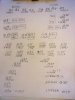
Here I am posting a diagram of the arrangement of the transistors on the GWH-148 amplifier board. The view is from above FROM THE ELEMENTS SIDE !!! This can make it a lot easier for someone changing transistors. Another explanation: the Q numbers of the transistors as well as their designations are from the repair catalog and also from the actual designations on the transistors themselves that are actually mounted on the board. Where there is a change, the numbers of the transistors are enclosed with : / transistor number / . These are the transistors 603 and 115, both with a TO92 case, which are the actual ones on the board. The hFE of some transistors are enclosed in a rectangle. The data was taken from 5 Pioneer A9 amplifier boards.
TR VIEW UP.jpg
 
Last edited:
A picture of the GWH-146 board would be informative. The GWH-146 board mounts up against the back panel, am I correct?
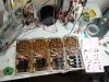
Sorry paying attention for this not in the wright moment. Are you mean GWH-148 ? If is this-Yes. This is the only big plate mounted on to the back plate with a soldering facing the back panel. So I remove it from the case of the amp and connect with extended wires every single connection to made accessible measuring in every point.(not shown here). Also attached to this the driver plates. Sure I will send pics right now here.Also forget to asking do you have a good service manual and good pictures of it? I got it om a files a photos of the original service manual and can sent to you if you provide me a email. Is 180 Mb . I send it already to Qsilver . 20220324_193509.jpg20220506_210518.jpg
 
transistor numbers are only supplied as intended replacements for malfunctioning originals.
GWH-146 was on the schematic I was using, paying closer attention I see more GWH-148's on other schematics.
I eventually found pioneer GWH-146 pictures on ebay (but never any gwh-148) that matched closely with the service manual.
I wanted to see how tightly packed it was, if there was room for some heat sinks on the 1/2 watt dissipating transistors.

I surmise we are starting out looking at voltages on the working board.

I have to keep on reminding myself that the 75 ohm resistors on the driver emitters are located on the GWX-593 & GWX-594 boards.
which you plug in to whichever board you are working on.
 
I have an A-9 that I've replaced these transistors on. I fitted them at almost maximum distance from the PCB that the legs would allow me. I didn't add heatsinks because I found that if I did, the biasing would tail off as they warmed up. Setting the idle was very difficult and very sensitive to ambient temperature - more than other NSA's like the SA-8800.

Everything runs quite hot... The regulator board next to the power amp PCB runs are close to 200°F. Don't like that either...
 
transistor numbers are only supplied as intended replacements for malfunctioning originals.
GWH-146 was on the schematic I was using, paying closer attention I see more GWH-148's on other schematics.
I eventually found pioneer GWH-146 pictures on ebay (but never any gwh-148) that matched closely with the service manual.
I wanted to see how tightly packed it was, if there was room for some heat sinks on the 1/2 watt dissipating transistors.

I surmise we are starting out looking at voltages on the working board.

I have to keep on reminding myself that the 75 ohm resistors on the driver emitters are located on the GWX-593 & GWX-594 boards.
which you plug in to whichever board you are working on.

Okay. I'm just now warming up to what you're talking about. You are exactly right! All my boards are also 146. I hope there is no big difference in the scheme of 148 and 146. Yes , measuring the voltage of the GWH-146 in the places you indicated according to #51. Yes, the GWX-593 and GWX-594 split-in-two 2X75 ohm R1 and R2 driver boards and this amp are the setup we're testing the GWH-146 boards on. I am currently soldering transistors Q9-Q16.
 
I have an A-9 that I've replaced these transistors on. I fitted them at almost maximum distance from the PCB that the legs would allow me. I didn't add heatsinks because I found that if I did, the biasing would tail off as they warmed up. Setting the idle was very difficult and very sensitive to ambient temperature - more than other NSA's like the SA-8800.

Everything runs quite hot... The regulator board next to the power amp PCB runs are close to 200°F. Don't like that either...

After the transistors heat up and after the change, then what is the logic of changing them at all. At least some of them are known to have worked for 40 years. Could it be that the cause of the overheating is not in the transistors but outside them? For example, by a strong current to them or to amplify some parasitic high frequency. There may be a root cause Not on all amplifiers these transistors are equally hot. On my working amplifier Q9, Q10 are not hot, Q11,Q12 are hotter and only Q13,Q14 are hot. But on all broken amplifiers, all these transistors overheat . There should be some reason for this
 
I also do not think there are many differences between the GWH-148 and GWH-146 boards.


But on all broken amplifiers, all these transistors overheat . There should be some reason for this

There is. we just haven't found it, yet. Different voltages mean different currents flowing, some currents are enough to smoke out resistors.

The transistors if NOT initially damaged, are definitely not improved with the greater heat exposure.
Save the originals (record exactly where they came from), if we blow up replacements, when we are completely finished and all is understood about the repairs, they can easily go back in.

I'm trying to establish a sequence of voltage tests to find which sections to fix first. This was started by changing the 150 ohm resistor to a pair of 75 ohm resistors to get a reasonable feedback source without the output transistors connected. With this reasonable feedback source on the older NSA amps I would then get the system to correctly balance the output at 0.000v.
Without the feedback, the amp would slam into either the positive rail or the negative rail. Very difficult to find fixes under those conditions.
Then at least when we find the OTHER reason for that amp being "railed" and fix it, the 0.000v will tell us of our success.

Everything from Q1 through Q29 & the Q1 driver have to be working correctly for the amplifier to balance at 0.000v

Back on post #43, I drew an orange "box" around a group of circuits, Q25 & Q27 (Q26, Q28) . They are current sources, and we check them along with Q7 & Q15 to see that they are working correctly. All four (q7, q15, q25, q27) are current sources / sinks that operate independently (almost) of the amp' feedback loop.

how? Voltage readings: emitter base and collector.
I am going to use an easier one as an example, the Q7 current source:
R13 (6800 ohms) is connected to -60v and to the emitter of Q7 at -19.2v, 19.2v across 6800 ohms = 2.82 milliamps current.
R11 (22k), D1 & R9 (10k) are connected between -60v and ground, and the junction of D1 & R9 sets the base bias voltage, which should be -18.6v under proper operation. In other words the base voltage is 0.6v more than the emitter voltage on this NPN transistor..


the next transistors Q9 & Q11 (q10, q12) and their heat dissipation are set by just a 10,000 ohm resistor and are not easily disturbed.

Then we check Q15 (Q16) for proper operation. .
Q15 is a npn transistor, with emitter at -58.7v, through R37 100 ohms to the -60v rail. 60 - 58.7 = 1.3v across 100 ohms is 13mA.
(heat is 0.013a x (emitter v 58.7 - collector v 1.9) = 0.738w)
R35 (220), D3 & R33 (22k) are connected between -60v and ground, and the junction of D3 & R33 sets the base bias voltage, which should be -58.1v under proper operation. In other words the base voltage is also 0.6v more than the emitter voltage on this NPN transistor..


Q15 feeds the NSA stage of q17, q19, VR1, STV-4H diode, q21, q23 which develop the positive and negative base voltages to run the pre-driver / driver / output transistor string.
Q25 & Q27 set the operating points for q17 & q19 (Q25) on the positive side and q21, q23 (Q27) on the negative side. Q13 is the other half of this stage and carries in the audio.

Q25 is a pnp current source and Q27 is an npn current source.
They share the base biasing scheme, R51 (1.3k) R55 (47k) VR3 (100k) R53 (1.3k) connected between the +60v and -60v rails.
Q25 emitter is connected to +60 through 1000 ohms.
Q27 emitter is connected to -60 through 1000 ohms.
Their collector outputs are connected together by a string of diodes and resistors: R101 (100) D11, D13, D15, D17, R103(100).
Their currents should be the same due to the resistor values and shared biasing arrangement.
The test is that the emitter voltage is 0.6v less than the base voltage.
Accuracy in voltage readings is enhanced by using the -60v rail for black dmm lead for npn transistor Q27, and +60v rail for black dmm lead for PNP transistor Q25.
power dissipation is calculated by (R47volts / R47 ohms) milliamps x (Q25 emitter voltage - Q25 collector voltage.)

Get this circuitry working, and finding a pre-driver or driver fault when it's being fed the correct base voltage becomes considerably easier. This base drive voltage also determines the heat being pushed through those transistors and emitter resistors.

One COULD fall back on "old tried and true", checking every resistor out of circuit, every capacitor out of circuit, every diode and transistor in a smart tester.

Now, that's a heck of a load, it's not intended to be digested in one lump, but rather to break it down in small sections and be studied. I hope I have spotted and fixed all the typos.

 
Last edited:
Thank you Mark for the extensive and detailed explanation. I think I understand exactly what we are doing. Some things from the last post I need to read more carefully to understand them. Reminds me of something about tuning fork 2. I'm still on No. 51. Before starting, I set all Vr to 0.2-0.4 Ohm. Then I started the usual test of the amplifier board with the voltages given on the service schematic. A quick check to make sure we don't make false measurements.. There is a discrepancy. Still at the beginning. Preliminary rough data - on the full - tomorrow.

Q9,Q10- difference 20%

Q11,Q12 – difference 20%
Q13 …B+57 ..C+10.84…E +55.8
Q15…E…-60…C…-0.9
Q16…E…+56, C…-3.7
Q14 E+56.2 …C…+5.9 B…+58
More- Q41 pin2 …-0.085 , pin7…+0.385 , pin 4 and pin 8 …+/-14.2
The emitters of the drivers on the left channel are -1.4 and -2.9V / On the right channel they are +/-1.5V
Here I did an experiment - I touched the thermal sensor of the driver board on the right channel to the hot solder of Q13 until it heated up to about 50C and measured the voltages on PT of the right channel they were in absolute value E..0.004 , C ..59, B..0.625 !!! That is, the base voltage immediately changed from -2.4 Volts to -0.625 Volts and with increasing temperature I think it will stay somewhere there but I could not stand the heat and let it go - after a few minutes the voltages returned to their unfavorable form in which I had them post - B=-2.4 volts. I repeated this several times and the result was the same. I will continue tomorrow. And may be will extend the wires from thermo sensors to attach them with insulation band to the hot soldering of the transistors to imitate the heat of the heat sink made from the bias
 
"...Save the originals (record exactly where they came from), if we blow up replacements, when we are completely finished and all is understood about the repairs, they can easily go back in...."
Thank you Mark! It hit me right on the nostalgia of 1980. That's what I wanted to hear. Now I can change any transistors without any worries
:))
 
One of the measurement conveniences I use, is to use the output (it is the feedback point too) point of the amp as the black dmm reference when I am measuring the push pull driver circuitry. Then with a significant DC offset from ground (+0.3v) the ground referenced readings may be, for example, +2.1v and - 1.5v while actually +1.8v and -1.8v is being delivered to the pre-driver transistors.

Soldering iron temperatures delivered to a transistor are well outside of their operating conditions. Possibly even damaging.
Please don't set yourself up with a red herring.

The emitters of the drivers on the left channel are -1.4 and -2.9V / On the right channel they are +/-1.5V

One thing to pay close, careful attention to is the base to emitter voltage on each driver. When it is not similar to the Vbe voltage of about 0.6 volts there is a problem with that transistor.

Q13 is a bit "too far back" to be affecting the magnitude of the driver voltage. It's function is to deliver the audio to the NSA circuitry, which splits the audio into two streams of different voltages, controlling the positive and negative halves of the push pull drivers.

. Assuming that Q15 is delivering the correct current, the components that set the driver voltages above and below the output voltage are Q17 & Q19 for the NPN positive side drivers (Q29, and GWX-593 Q1) and Q21 & Q23 for the PNP negative side drivers (Q31, and GWX-593 Q3).
An overall rule of thumb for the NSA circuit output driver voltages is that they should be roughly symmetrical at rest.
And be 3 x Vbe's in magnitude.
pre-driver Q29: Vbe #1 (1.8v to 1.2v),
driver GWX-593 Q1: Vbe #2 (1.2v to 0.6v)
multiple output transistors in parallel: Vbe #3 (0.6v to 0.0v).

a side note: tomorrow I have a significant Physican's appointment, so I will be absent at some point for an unknown interval.
 
Last edited:
As a baseline, it would be a good idea to measure and record the dc offset voltages and idle currents of your good, reference board.

Once new trimpots for vr1- vr4 are installed (*), a second check to see if there are idle currents flowing at full CCW ( zero ohms) would be a good idea.

* ( on the belief that you found problems with even the reference board's trimpots.... iiac )
 
Back
Top Bottom