• The move to the new server is done. There are some software and database maintenance updates in process. This has us passing the hat around to help out. We appreciate any donations. Seriously, even a dollar helps. The payment page may be found here - https://www.audiokarma.org/support.html

Repair Pioneer A9 NSA

"Just in case, I gotta ask; When doing ohmmeter readings, the power is turned off?"
Yes.After every measurement power OFF, Discharging the big capacitors with 200 Ohm resistor and after that , shorting them. And before every turn ON first DBT until the light go to dimming and than plug into 120 V and measure on 120V.
So what we should do with this plate if has no issues . I just finishing the other measurements with variation with a VR1/VR2 on 4 stages from 0 to 100 Ohms and just stuck into the MS Exel to post the results , but will take a time. If we need it. The base voltage is regulating from 1.6V to 1.985 v for each channel.
To connect the next plate with a problems? There 3 more left.
 
First: good procedure.Good for discharging, then shorting caps.

If the other three "plates" were on my bench, I would do things a bit differently. I have desoldering equipment that makes it very easy and quick for me to pop out a transistor, then test it. I would look carefully around each removed transistor for damaged companion resistors.
That way power on testing becomes much more of a formality to ensure that I missed nothing.

My attitude could be summed up: "until proven good by myself, EVERYTHING is considered busted.

Live testing would first verify current sources and sinks Q7, Q15, Q25, Q27. Then I would look at the base voltages being sent to the Q29 & Q31 drivers
 
First: good procedure.Good for discharging, then shorting caps.

If the other three "plates" were on my bench, I would do things a bit differently. I have desoldering equipment that makes it very easy and quick for me to pop out a transistor, then test it. I would look carefully around each removed transistor for damaged companion resistors.
That way power on testing becomes much more of a formality to ensure that I missed nothing.

My attitude could be summed up: "until proven good by myself, EVERYTHING is considered busted.

Live testing would first verify current sources and sinks Q7, Q15, Q25, Q27. Then I would look at the base voltages being sent to the Q29 & Q31 drivers

"until proven good by myself, EVERYTHING is considered busted.”I agree with this motto. The knowledge gained from experience over the years is priceless and usually "it's not in the books".

I proceed in a similar way -the three boards are free floating connected by extended connectors and are easily separated. Now the temperature of the driver transistors has dropped. Q11 to Q16 are hot. Not like before up to 80C, but they are around 50C-60C measured with a finger. :)
“Live testing would first verify current sources and sinks Q7, Q15, Q25, Q27. Then I would look at the base voltages being sent to the Q29 & Q31 drivers”
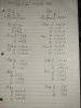
On Q1-Q16 without Q5, Q6 the voltages are given in the service description. But the pre-drivers Q29-Q32 are not given. What we measured for them in these tables with the variation of VR 1,2,3,4, is that what it should be and can it be a reference for comparison?
From here on, what is the way. My plan was now to disconnect this board and attach the next one for repair, then on the repaired boards I would install them on the amplifiers with a checked power supply again. First without PT and if they are OK, put the drivers with PT. And then setting the DC offset and bias. Is this OK?
 
The GWH-146 board that we have made so far is on amplifier number 4. I removed it and in its place I put the amplifier board GWH-146 on the amp. Number 1.
This board has much more damage it seems. The same parts have been replaced on it as in the previous one. The voltages are of course not good. This is where I post the voltages according to #87 "Live testing would first verify current sources and sinks Q7, Q15, Q25, Q27. Then I would look at the base voltages being sent to the Q29 & Q31 drivers"20220721_015554.jpg
 
I have not dug as deeply as possible into these numbers,

I think the Q8, Q10, Q12, Q14, Q16, Q30 & Q32 channel is good,

The other channel, the Q7 current source looks ok
Q9 & Q11 present the appearance of circuits striving mightily to correct a downstream fault that has railed that channel.
I blame that on Q13.
Does Q13 pass a function test? it is supposed to be a 2sa905. put a ksa1381 or ksa1142. There is no reason to prefer the 1381 or prefer the 1142. Just presenting you with alternatives.

Once Q13 has a substitute installed, repeat the Q7, Q9, Q11, Q13,Q15, Q29 & Q31 voltage measurements. That will tell us if we made progress, and what else may be damaged by the railed amp channel.

In other words, if that doesn't completely fix it, don't be discouraged, we are IN the process.

my next suspect is Q15, 2sc1915 subbed by KSC3503 & KSC2682.
If there's not +/- 1.6v on the bases of Q29 & Q31, try substituting Q15.

I can't dig deeper on Q15 to see if there's a fault,
your emitter and base data lists e -60, b -60
yet the Q16 data lists e -60.65, b -60.12 which I can work with..
 
Last edited:
I have not dug as deeply as possible into these numbers,

I think the Q8, Q10, Q12, Q14, Q16, Q30 & Q32 channel is good,

The other channel, the Q7 current source looks ok
Q9 & Q11 present the appearance of circuits striving mightily to correct a downstream fault that has railed that channel.
I blame that on Q13.
Does Q13 pass a function test? it is supposed to be a 2sa905. put a ksa1381 or ksa1142. There is no reason to prefer the 1381 or prefer the 1142. Just presenting you with alternatives.

Once Q13 has a substitute installed, repeat the Q7, Q9, Q11, Q13,Q15, Q29 & Q31 voltage measurements. That will tell us if we made progress, and what else may be damaged by the railed amp channel.

In other words, if that doesn't completely fix it, don't be discouraged, we are IN the process.

my next suspect is Q15, 2sc1915 subbed by KSC3503 & KSC2682.
If there's not +/- 1.6v on the bases of Q29 & Q31, try substituting Q15.

I can't dig deeper on Q15 to see if there's a fault,
your emitter and base data lists e -60, b -60
yet the Q16 data lists e -60.65, b -60.12 which I can work with..

Q13 is KSA1142-Y. I de soldered it, measured it hFE=288. I replaced it again with the same type. From Q9-Q16 and Q29-Q32 are new transistors for the respective correct positions KSA1142/KSC2681 and the predrivers are KSA1381/KSC3503. I measured the voltages again and they are the same as in #90. Should I start testing with a fluke all the elements on the faulty and working board and compare them, unplugged of course with a presumption to find leaking diode or shorted capacitors or burned new transistor?
 
considering that the transistors (Q29) are ok, check or replace D27.

i'm looking at where the 60v can come from.

could you indulge a functional test of Q29 & Q31?
transistors don't like Base to Emitter voltages of 5 volts and larger magnitude.
they could be zapped already.
 
They has the same reading tested with a Fluke on diode tester on the defective board and on a reference board. But let me pulled out to make the rel test out of the board. It is ok to test also D5 zener with a 800Ohms and 60 volt batery to see the voltage that provide?
 
There is some contradictions about looking up that zener online. I don't think it's a 27 volt, 55 mA device.( 3 or 5 watts!!)
The physical size for such a powerful device is significantly larger than the 1n4148 type glass diodes. The pictures don't support that idea.
So I think 60v and 800 ohms could be significant overkill.

I'm thinking 5mA current for a 2.7v 0.5w zener diode (78-BZX55B2V7 : 2.7v 2% tolerance) so 9v and a 1800 ohm resistor.
if it is 27 volts, 60v and a 6000 ohm resistor limits to 5mA (0.150w) , worst case if a low voltage zener gets wired in would get 10mA, that might be a bit high.

2.7v more corresponds to what is drawn into the schematic. 60v - 57.4v = 2.6 volts.

I did check the tuning fork to see if there was anything about sz(-027) type diodes. nope...

Caution is often rewarded.
 
Last edited:
The zener D5/D6 are SZ-027 . I already removed and tested with a chinese tester. It shows me zener voltage 2.45V other same zener from another board 2,7V , another one from the other channel 2.43V. So This zener should be 2.7 volts and is ok By accident I did not toasted them whit 60V because this time I start reading before to acting. So I replace this zener with the zener D6 from another board that is still not in the game.The predrivers KSA1381/KSC3503 I removed and tested. They are ok but the hFE is changed. Before installation was KSA/KSC=120/80 and now is KSA/KSC=89/84. I replaced them again with a fresh one . They are Onsemi from Mouser. The diode D27 is ok tested with a fluke and diode tester .Forward voltage =0,545 ,reverse voltage=insulator .Also the emitter resistor for Q29 has a crack and under the resistor on the board is dark spot. I stil 100 Ohms Will be changed . There are broken lines on the board and I have to solder wires from point to point. Let do this and i will measure again.
 
I connected everything and measured. The left channel is consistently bad and keeps the voltages with a deviation from the posted sheet in #90 with -/+0.2 volts. On the D5 zener I measured 2.7 volts with the probes at both ends. Also at both ends of D27 it was almost the same around 2.7 volts. On D31/D32 +15 volts. On Q1 +15 volts on Q2 +2.5 Volts. The supply voltage is unbalanced -62 volts to +59.9 volts. -38/+32 volts through DBT. Big difference in the voltages of the field effect transistors Q5/Q6 - no data about them but I can measure from the repaired board.
I did another test - I disconnected all the connectors and left the board only on power and ground. The supply voltage became symmetrical: -/+58.5 volts. I remeasured all the voltages in this position and they fully correspond to those listed in #90 with one exception - negative voltages appeared on the minus terminal for the speakers. On the left channel -58 volts, and on the right -25 volts. I think I had such a problem at the beginning and I don't remember how it was solved because it disappeared when we connected everything and made a middle point on R1/R2 with 2x75 ohms. May be ground is lost somewhere. I'll check all the cables now. What could it be? Interesting thing was that in the very first connecting to the amp. This board was almost ok and the amp turn down the protection , and after 20 minutes turned on the red light and go to protection mode.. Let check the cable to be sure that is not something stupid problem.
 
I carefully checked the cables from the GWX-593/594 driver boards to the GWH-146 amplifier board and also all the solder joints and tracks. I found no short circuit or open.
 
I think I had such a problem at the beginning and I don't remember how it was solved because it disappeared when we connected everything and made a middle point on R1/R2 with 2x75 ohms.

that's easy... without the output transistors the middle point was disconected and "floating"...when we made the artificial middle point that was fixed temporarily.

without the pairs of 75 ohm resistors you added on the GWX-193 & GWX-194 the feedback loops that you established for operating without output transistors has been broken. The middle point is again "floating".

keep Q29 (Q30) & Q31(32) connected but have a pair of (about) 340 330?) ohm resistors substituting for R61's 680 ohms (other channel R62) and the center (artificial middle point)
of the two resistors connected to R71 8.2 ohms, 2 watts, the side AWAY from the C25 0.033uF capacitor. On the other channel it is R72 and C26.

THEN you will be able to operate the board.

The other thought I had (and rejected) is to remove Q29 & Q31 but there is a can of worms to deal with, the feedback has an impedance of 20,000 ohms and Q29 & Q31 bases are connected to R59 (2.2k) with thermistor th1 in parallel with R59, then in series with R57 (6.2k) for up to 8400 ohms between the bases..
The feedback may need more current than that hookup can provide.
In adding some splitter resistors between Q29 base and Q31 base this 8400 ohms would be diminished, and with the R43 and R45 220 ohm resistors the base voltages may be altered. Maybe not a lot, or maybe enough to cause other problems.

The fact that the negative voltage recovers with the other connectors removed suggests that there is a problem on those other boards that pulls heavily upon the -60v power rail.

What are the other boards, also how are you getting power in? GWR-141? (only?)

also when you can, please measure and post the Q13 voltages, looking for 0.1v or greater differences between the base and emitter voltages.

On the GWR-141 board, R1 (10 ohms) positive side and R2 (10 ohms) negative side can be voltage measured across itself (red dmm one side, black dmm other side of the same component at the same time) and ohms law used to reveal the current draw for each.
1.0 volt across 10 ohms is 0.100 amps or 100 Milliamps.
+60v is supposed to be pulling 0.100 amp
-60v is supposed to be pulling 0.069 amp

.
 
Last edited:
that's easy... without the output transistors the middle point was disconected and "floating"...when we made the artificial middle point that was fixed temporarily.

without the pairs of 75 ohm resistors you added on the GWX-193 & GWX-194 the feedback loops that you established for operating without output transistors has been broken. The middle point is again "floating".

keep Q29 (Q30) & Q31(32) connected but have a pair of (about) 340 330?) ohm resistors substituting for R61's 680 ohms (other channel R62) and the center (artificial middle point)
of the two resistors connected to R71 8.2 ohms, 2 watts, the side AWAY from the C25 0.033uF capacitor. On the other channel it is R72 and C26.

THEN you will be able to operate the board.

The other thought I had (and rejected) is to remove Q29 & Q31 but there is a can of worms to deal with, the feedback has an impedance of 20,000 ohms and Q29 & Q31 bases are connected to R59 (2.2k) with thermistor th1 in parallel with R59, then in series with R57 (6.2k) for up to 8400 ohms between the bases..
The feedback may need more current than that hookup can provide.
In adding some splitter resistors between Q29 base and Q31 base this 8400 ohms would be diminished, and with the R43 and R45 220 ohm resistors the base voltages may be altered. Maybe not a lot, or maybe enough to cause other problems.

The fact that the negative voltage recovers with the other connectors removed suggests that there is a problem on those other boards that pulls heavily upon the -60v power rail.

What are the other boards, also how are you getting power in? GWR-141? (only?)

also when you can, please measure and post the Q13 voltages, looking for 0.1v or greater differences between the base and emitter voltages.

On the GWR-141 board, R1 (10 ohms) positive side and R2 (10 ohms) negative side can be voltage measured across itself (red dmm one side, black dmm other side of the same component at the same time) and ohms law used to reveal the current draw for each.
1.0 volt across 10 ohms is 0.100 amps or 100 Milliamps.
+60v is supposed to be pulling 0.100 amp
-60v is supposed to be pulling 0.069 amp

.


UPS. sorry Mark, yesterday I didn't get a post and because I was impatient I did something that is probably stupid because it doesn't count the overall functioning of the board. And I think I posted it last night when it still didn't have your reply post, but for some reason my post didn't show up. Anyway, I'm posting it now to update you on what I've done and what the status is now with the transistors removed. From here I can put them back on the board and follow this instruction #99. Or if you think you can use some of what I've done. I'll wait for yes or no.

So, this is the post that should have appeared before #99 but it didn't. I'm posting it now:

*
To find out if the problem is in a transistor or not, I started to remove the transistors and make a quick measurement of only the power supply and ground (the voltages are almost the same for Q13 as when all the connectors are fully connected). My goal is to see when on Q13 C-56.3 volts will disappear or change.. Currently I have removed all transistors on the left channel from Q1 to Q32 except Q15 and when powering the board with -/+60volts and ground voltages of measured in the holes of transistor Q13 the C-56.3 V is still there. This voltage is changed when I removed Q15. When I re installed Q15 the voltage on Q13 e=-56.3V come back. I don’t know it is will help to find the problem. All removed transistors are OK.I changed D27 but no difference,

I tested the same way another amplifier board GWH-146 with fully removed transistors. The voltages into the hole of transistors are symmetrical and with closed value So keep looking where is the problem *
 
What are the other boards, also how are you getting power in? GWR-141? (only?)


.[/QUOTE]
On GWH 146 is powered true CN2 connector with -/+60V from AWR-226 regulator board and the ground terminal on opposite side of the board point 25/26 are connected to the chassy where are connected every single ground cables including the ground from the big caps.The other boards are all the boards which are normally connected to the amp. board GWH-146
Just info There is 58 V true R71
I understand that without transistors the diagnosis cannot be correct. But at least I checked all the transistors that they are ok. Also could a bad solder on Q15 be the cause?
 
Last edited:
we shall continue once the post #99 tests are completed. Readings like done in post #90 are also needed. Even if they are all good - a baseline is needed.

Also could a bad solder on Q15 be the cause?

YES, absolutely.

A bad solder joint on Q15 collector would do nasty things.

One way to imagine the circuit is a series of springs, under tension.
one spring Q13 is anchored to +60v, the other spring Q15 is anchored to -60 volts.
they are connected by some components, and everything is under tension.

If the spring or a component breaks,
everything on one side of the break is pulled to +60v
everything on the other side of the break is pulled to -60v
chaos and carnage ensues.

It is the same with the Q25 & Q27 control circuit.

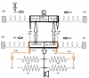
I also added to the drawing the pre-drivers Q29 & Q31, the Q1 & Q3 drivers and the Q1, Q2, Q3, Q4 outputs as well as the resistors to show the actual middle point and how it eventually affects the NSA control circuits (Q25 & Q27).

upload_2022-7-23_22-34-47.png
 
Last edited:
we shall continue once the post #99 tests are completed. Readings like done in post #90 are also needed. Even if they are all good - a baseline is needed.


YES, absolutely.

A bad solder joint on Q15 collector would do nasty things.

One way to imagine the circuit is a series of springs, under tension.
one spring Q13 is anchored to +60v, the other spring Q15 is anchored to -60 volts.
they are connected by some components, and everything is under tension.

If the spring or a component breaks,
everything on one side of the break is pulled to +60v
everything on the other side of the break is pulled to -60v
chaos and carnage ensues.

It is the same with the Q25 & Q27 control circuit.

I also added to the drawing the pre-drivers Q29 & Q31, the Q1 & Q3 drivers and the Q1, Q2, Q3, Q4 outputs as well as the resistors to show the actual middle point and how it eventually affects the NSA control circuits (Q25 & Q27).

View attachment 2622481
Thanks for the nice and clear explanation. This diagram is a very important clarification. Now I understand how stupid I was to think that the damage must necessarily be a burnt element. In fact, the circuit is made of active elements and must be symmetrical and in equilibrium at certain values of the voltages. Hopefully we can achieve this balance in the schematic and on the board. Now I will carefully re-solder the transistors. Those that are ok but have reduced their hFE, I replace them with new ones again (I don't know if this means they are counterfit, I bought them from Mouser). I have already checked all the diodes, zeners, emitter resistors and capacitors. I also have 330 ohm resistors. And I will process #99 and #90
 
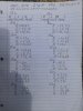
1 146 v.jpg I measured the removed transistors Q1-Q31 and noted at what position what hFE they are. I replaced Q9 KSC2682-Y with a new one again because it had reduced hFE. (new transistors should not have such a drift, but some of them when they work at 60 volts and drifted .I wonder if they are quality transistors ). There is a positive change, unknown from what - maybe a bad solder. Know it may be necessary to somehow balance the voltages according to No. 102. I post the measurements as in #90 and prepare for #99.
 
A lot of post 99 is mostly concerned with making another resistor split point for when the GWX-593/594 boards and THEIR added split point have been disconnected. Also, to be clear, only ONE split point (per channel) should be in use at any particular time.
IF you do not contemplate operating without the GWX-593/594 boards, the additional 330 ohm modifications will not be needed.

The rest of post 99 was concerned with the negative power supply and it's possibly excessive loading.

ok.now:

The results posted in #104 are at first glance good except for Q31 & Q32 at the end.
Q31 base at -1.26v, emitter at -2.105v
Q32 base at -1.22v, emitter at -2.12v

The expected result would be that the emitters are at a lower voltage than the bases, like for Q29 (+1.66v, +1.54v) and Q30(+1.76v, +1.56v)

Have you done anything to R61 & R62 to establish an artificial split point?

edit: looking closer says not so fast....
 
Last edited:
Back
Top Bottom