• Please note that Audiokarma will be offline briefly for updates early on Monday morning, September 28th.

Repair Pioneer A9 NSA

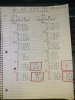
Q15 correct.jpg
A lot of post 99 is mostly concerned with making another resistor split point for when the GWX-593/594 boards and THEIR added split point have been disconnected. Also, to be clear, only ONE split point (per channel) should be in use at any particular time.
IF you do not contemplate operating without the GWX-593/594 boards, the additional 330 ohm modifications will not be needed.

The rest of post 99 was concerned with the negative power supply and it's possibly excessive loading.

ok.now:

The results posted in #104 are at first glance good except for Q31 & Q32 at the end.
Q31 base at -1.26v, emitter at -2.105v
Q32 base at -1.22v, emitter at -2.12v

The expected result would be that the emitters are at a lower voltage than the bases, like for Q29 (+1.66v, +1.54v) and Q30(+1.76v, +1.56v)

Have you done anything to R61 & R62 to establish an artificial split point?

edit: looking closer says not so fast....
"Have you done anything to R61 & R62 to establish an artificial split point?"

No nothing.This is de corrected post with areal voltage Q15 C
View attachment 2624024 But since you mentioned them I decided to check them out because it was in this area of Q29 and Q31 that the board was badly damaged and I had to replace stripped and broken tracks with wires. One solder on Q29 E to R61 was bad and I re soldered it.(marked with a star on the sheet) This caused the voltages to change and shifted the voltage balance point to new position according to #102. Maybe better . Here I post the change of voltages that was obtained after re-soldering the emitter of Q29 to the track of R61. Values enclosed in red lines are the current latest results.

Now we will take a closer look at how to proceed #99.
 
Last edited:
I got a little confused here. Is the whole procedure in #99 as far as I understand is to create a load and close the feedback loop in order to remove the voltage on the minus terminal of the speakers output?
 
procedure 99 is just a repeat what you did in post 47, create an artificial center point when the real center point was lost due to no output transistors being connected. It would be the plus terminal of the speaker output. The minus speaker terminal is just a ground.

The difference is that it is intended to actually be on the GWH-146 board, instead of on the unplugged GWX-593/594 boards. When unplugged, kludge #47 isn't connected and providing feedback.

That feedback connection allows the amplifier circuits to balance itself. That connection almost always is the output of the amplifier, before the series inductor or zobel filter (R71 9.2 ohms, C25 0.033uF) & (L1 1.3uH R87 10 ohms 2 watts)
When working correctly there are a LOT of symmetrical voltages.
And YES, with the changes I specified, the zobel filters ARE connected.

The q29 q30 q31 q32 voltages look much much better.

I am HOPING that Q15 collector is a typo, and it's more like -1.73v, other data in the table suggest that.

my concern is that the
collector voltage of Q13 is connected with R43 a 220 ohm resistor to Q29 base : q13C = +5.54v q29B = +1.65v
collector voltage of Q14 is connected with R44 a 220 ohm resistor to Q30 base : q14C = +5.38v q30B = +1.63v

collector voltage of Q15 is connected with R45 a 220 ohm resistor to Q31 base : q15C = -17.23v typo? q15c = -1.723v q31B = -1.26v
collector voltage of Q16 is connected with R46 a 220 ohm resistor to Q32 base : q16C = -1.73v q32B = -1.63v


The pattern is repeated from Q13 to the other channel's Q14, +5.54v versus +5.38v. dropping down to +1.65v versus +1.63v , across a single 220 ohm resistor. That implies a lot of current. D19 the 2.2v zener diode comes to mind as a safety limiter. (6.54 - 1.65 = 3.89v 3.89v / 220 = ~17.7mA....
while the Q16 (neglecting q15's typo) collector is -1.73v to Q32 base -1.638v are good voltages.

Thus I am casting doubt upon the Q17, Q19, R39 circuit. Please check (power off) the circuit connections.
when I do not trust a connection, I measure the ohms from component lead to component lead,
thus any bad solder joints or interrupted pc board paths are revealed.
for example, (all are "zero ohm" paths):
Q13 collector to Q17 collector
Q13 collector to R39
Q13 collector to R43
Q17 emitter to VR1
Q17 emitter to Q19 collector
Q17 base to R39
Q17 base to Q19 emitter
Q19 base to Q25 collector
Q19 base to R101

I will be digging deeper when I am fresh tomorrow, my eyes scream for sleep.

We may end up taking readings of Q17, Q19, Q25, Q21, Q23, Q27, and the other channel Q18, Q20, Q26, Q22, Q24, Q28,
to diagnose.
 
Last edited:
"I am HOPING that Q15 collector is a typo, and it's more like -1.73v, other data in the table suggest that."
Yes . Sorry. Q15 C= -1,743 quick fresh checking. Will correct the page .


What I figured out was to replace R61(L) and R62(R) with two 340 ohm resistors each and connect the midpoint of the new resistor pair to R71(L) and R72(R) at their points away from C25(L) and C26(R).


What I think I understand about the procedure in #99 is that in this way the driver boards GWX-593/594 with the previously created midpoint ,can be disconnected, and the new circuit allows the board to self-balance its voltages and somehow we can make corrections to striated up the right voltages. The old coupling did not provide such self-balancing.
And should this be done only for one channel at the time?
Just for info :
Know the voltages on the output terminal are:
On the positive terminals L/R = -0.004V
Negative R=0.000V
Negative L=+0.001V !
Is this positive voltage on the negative terminal is possible bad ground or is something else?
 
Last edited:
"
Thus I am casting doubt upon the Q17, Q19, R39 circuit. Please check (power off) the circuit connections.
when I do not trust a connection, I measure the ohms from component lead to component lead,
thus any bad solder joints or interrupted pc board paths are revealed.
for example, (all are "zero ohm" paths):
Q13 collector to Q17 collector
Q13 collector to R39
Q13 collector to R43
Q17 emitter to VR1
Q17 emitter to Q19 collector
Q17 base to R39
Q17 base to Q19 emitter
Q19 base to Q25 collector
Q19 base to R101"
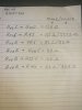
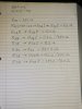
The result of this measurements are in the attached **** below. The resistanceOhms.jpg of the shorted probes is 0.1 Ohms
 
I've been working on a post. I stored it for now. It would be confusing in this context.

I see the numbers and results from the tests.

I realize I was not complete:

R39 needs verification of 750 ohms
one side of R39 connected to R43 & Q13 collector
the other side Q17 base and Q19 emitter

thus
R39 to Q13 collector
R39 to Q17 collector
R39 to R43
---other side of R39 -----------
R39 to Q17 base
R39 to Q19 emitter.

I am sorry for that omission (last night (yawn))

the overall reason is that in the schematic Q13 collector is showed at +1.9v instead of the +5.5v or so you that you measured.

Between this +5.5v at Q13 collector and ~ +1.6v at Q29 base is only R43, that 220 ohm resistor.
The search is on to find out why that voltage is so high, and HOW is it being cut back to the lower voltage.
 
Last edited:
this is the clarifying post, responding to #109

I 'll try to clarify.

The amplifier has a differential input stage that has "non-inverting" and "inverting" inputs.

The overall amplifier has "feedback", sampled directly from the output (that will go to the speaker).
and connected back into the first (differential) input stage at the "inverting input".

So when, lets say, the input gets an ac varying voltage whose instantaneous value is 0.075v (a loud sound, 0.150v
is considered maximum for a "line level" input) the input stage will do "things" to get 0.075v at the output.
When it reaches 0.075v the feedback will cause it to freeze (balance) at those conditions.

Now a power amp with a gain of one (0.075v in, 0.075v out) isn't very useful.
So, how about a gain of 200? That turns 0.075v to 15 volts, and at 8 ohms that's twenty eight watts.
We get that gain by sending only 1/200th (0.075v) of the output voltage (15v) back to the inverting input (R107 20k & R19 100 )
to balance the system.
Viola!!!

Thus feedback is VERY important.

The feedback from a working amplifier is sampled at the output, which will eventually connect to the + terminal on the back panel.
This is found on the A-9 on the GWX-593(left) and GWX-594(right) boards in the form of R11(0.5 ohms) or R13(0.5 ohms) where their center taps are connected to the output to the speaker.

Now we add a complication. We want to operate (troubleshoot) WITHOUT the output transistors connected.
Thus R11 & R13 are disconnected from the transistors. There is NO feedback.

SO I added an artificial feedback point by replacing R1 150 ohms, with two 75 ohm resistors, and temporarily connected the center point
of the two connected 75 ohm resistors to pin 5 the output connection. Feedback is restored and the amp will again balance.

And thus we add ANOTHER complication - we disconnect the GWX-593 and GWX-594 boards!! All our feedback fixing work was ON THOSE boards...

So, I need a feedback point from Q29 & Q31. We replace R61 (680 ohms) with two 340 ohm resistors,
connect a wire to their center point, and go looking for a feedback connection. We find it at R71 (8.2 ohms)

IRONCLAD RULE FOR THE A-9 AMP: only ONE of the three possible feedback connection locations is to be connected at any time on a particular channel.
Now, remember - that's per channel, so there are two feedback points - one for the left channel and one for the right channel, for each of the three choices -
1. normal operation with output transistors (R11 & R13 / R12 & R14 0.5 ohms)
2. operation without output transistors. (R1 / R2 150 ohms)
3. operation without GWX-593 and / or GWX-594 boards.(R61 / R62 680 ohms)

Thus if / when GWX-593 and GWX-594 are reconnected, the connection to R71 / R72 MUST be DISCONNECTED.

When the output transistors are installed, the two 75 ohm R1 / R2 taps to the output (pin 5 or pin 10) also MUST be DISCONNECTED.

The measure of that doing "things" that I mentioned at the top is called "slew rate" and is defined as volts per microsecond.
 
Last edited:
I've been working on a post. I stored it for now. It would be confusing in this context.

I see the numbers and results from the tests.

I realize I was not complete:

R39 needs verification of 750 ohms
one side of R39 connected to R43 & Q13 collector
the other side Q17 base and Q19 emitter

thus
R39 to Q13 collector
R39 to Q17 collector
R39 to R43
---other side of R39 -----------
R39 to Q17 base
R39 to Q19 emitter.

I am sorry for that omission (last night (yawn))

the overall reason is that in the schematic Q13 collector is showed at +1.9v instead of the +5.5v or so you that you measured.

Between this +5.5v at Q13 collector and ~ +1.6v at Q29 base is only R43, that 220 ohm resistor.
The search is on to find out why that voltage is so high, and HOW is it being cut back to the lower voltage.

No problem, I'll measure what else I need, at least that's easy. And I work with this amplifier mostly at night in peace, Q14 C =+5.38V also, same likes Q13 and it is above the norm of 1.9 volts. Now I will make the new measurements.

About #99 I found in the drawer. 4 resistors small size like emitter resistors of 100 ohms which are 326 ohms each. I can add to them 10 ohms of the same size, maybe 1/4 watt, not sure.

If we replace Q13/Q14 with another transistor with less hFE will the collector voltage decreaseohms2.jpg
 
this is the clarifying post, responding to #109

I 'll try to clarify.

The amplifier has a differential input stage that has "non-inverting" and "inverting" inputs.

The overall amplifier has "feedback", sampled directly from the output (that will go to the speaker).
and connected back into the first (differential) input stage at the "inverting input".

So when, lets say, the input gets an ac varying voltage whose instantaneous value is 0.075v (a loud sound, 0.150v
is considered maximum for a "line level" input) the input stage will do "things" to get 0.075v at the output.
When it reaches 0.075v the feedback will cause it to freeze (balance) at those conditions.

Now a power amp with a gain of one (0.075v in, 0.075v out) isn't very useful.
So, how about a gain of 200? That turns 0.075v to 15 volts, and at 8 ohms that's twenty eight watts.
We get that gain by sending only 1/200th (0.075v) of the output voltage (15v) back to the inverting input (R107 20k & R19 100 )
to balance the system.
Viola!!!

Thus feedback is VERY important.

The feedback from a working amplifier is sampled at the output, which will eventually connect to the + terminal on the back panel.
This is found on the A-9 on the GWX-593(left) and GWX-594(right) boards in the form of R11(0.5 ohms) or R13(0.5 ohms) where their center taps are connected to the output to the speaker.

Now we add a complication. We want to operate (troubleshoot) WITHOUT the output transistors connected.
Thus R11 & R13 are disconnected from the transistors. There is NO feedback.

SO I added an artificial feedback point by replacing R1 150 ohms, with two 75 ohm resistors, and temporarily connected the center point
of the two connected 75 ohm resistors to pin 5 the output connection. Feedback is restored and the amp will again balance.

And thus we add ANOTHER complication - we disconnect the GWX-593 and GWX-594 boards!! All our feedback fixing work was ON THOSE boards...

So, I need a feedback point from Q29 & Q31. We replace R61 (680 ohms) with two 340 ohm resistors,
connect a wire to their center point, and go looking for a feedback connection. We find it at R71 (8.2 ohms)

IRONCLAD RULE FOR THE A-9 AMP: only ONE of the three possible feedback connection locations is to be connected at any time on a particular channel.
Now, remember - that's per channel, so there are two feedback points - one for the left channel and one for the right channel, for each of the three choices -
1. normal operation with output transistors (R11 & R13 / R12 & R14 0.5 ohms)
2. operation without output transistors. (R1 / R2 150 ohms)
3. operation without GWX-593 and / or GWX-594 boards.(R61 / R62 680 ohms)

Thus if / when GWX-593 and GWX-594 are reconnected, the connection to R71 / R72 MUST be DISCONNECTED.

When the output transistors are installed, the two 75 ohm R1 / R2 taps to the output (pin 5 or pin 10) also MUST be DISCONNECTED.

The measure of that doing "things" that I mentioned at the top is called "slew rate" and is defined as volts per microsecond.

Thanks for the detailed explanation Mark. Indeed, the strategy is very thorough. Now I have a general idea of what we are doing.This I have to learn more carefully. I still don't know how the voltage can be affected. Indeed, the situation here is quite complicated.
 
If we replace Q13/Q14 with another transistor with less hFE will the collector voltage decrease

Probably not. Because the +5.5v becomes about +1.6v on the other side of R43, it is hidden from the feedback system.

We need to take some more specialized voltage measurements. The specialization is that the black DMM reference lead will NOT be connected to ground, but rather to the positive 60 volt rail, to the negative 60 volt rail and to the output, the same place as the feedback is sent, R71 the amplifier output terminal.

VR3 is set to fully CCW
VR4 is set to fully CCW

DMM black lead to ground
Q13 emitter, base & Collector voltages
Q15 emitter, base & Collector voltages
Q14 emitter, base & Collector voltages
Q16 emitter, base & Collector voltages

DMM black lead to positive 60v rail
Q25 emitter, base & Collector voltages
Q26 emitter, base & Collector voltages

DMM black lead to negative 60v rail
Q27 emitter, base & Collector voltages
Q28 emitter, base & Collector voltages

DMM black lead to R71 or to ground if R71 voltage less than 0.003 volt different from ground.
Q17 emitter, base & Collector voltages
Q19 emitter, base & Collector voltages
(Q13 collector voltage, Q29 base voltage)
Q21 emitter, base & Collector voltages
Q23 emitter, base & Collector voltages
(Q15 collector voltage, Q31 base voltage)

DMM black lead to R72 or to ground if R72 voltage less than 0.003 volt different from ground.
Q18 emitter, base & Collector voltages
Q20 emitter, base & Collector voltages
(Q14 collector voltage, Q30 base voltage)
Q22 emitter, base & Collector voltages
Q24 emitter, base & Collector voltages
(Q16 collector voltage, Q32 base voltage)

DMM black lead to R71 or to ground if R71 voltage less than 0.003 volt different from ground.

While monitoring the Q19 base voltage, adjust VR3 by increasing resistance.
I don't know how to diagram this:

we want to discover if the full range of VR3 adjustment changes the Q19 base voltage.
what voltage the Q19 base starts out at VR3=0
is there a point where VR3 adjustment no longer causes a change in Q19 base voltage reading?
what voltage is the Q19 base when either you run out of potentiometer adjustment (full theoretical 100k) or the Q19 base voltage stops changing.

As the Q19 base changes, does any change occur to Q13 collector voltage ?
As the Q23 base changes, does any change occur to Q15 collector voltage ?


I'll just run with this for now.... post is finalized.
This post may not be finished, when this is removed,the post will not be added to, or edited.
 
Last edited:
Probably not. Because the +5.5v becomes about +1.6v on the other side of R43, it is hidden from the feedback system.

We need to take some more specialized voltage measurements. The specialization is that the black DMM reference lead will NOT be connected to ground, but rather to the positive 60 volt rail, to the negative 60 volt rail and to the output, the same place as the feedback is sent, R71 the amplifier output terminal.

VR3 is set to fully CCW
VR4 is set to fully CCW

DMM black lead to ground
Q13 emitter, base & Collector voltages
Q15 emitter, base & Collector voltages
Q14 emitter, base & Collector voltages
Q16 emitter, base & Collector voltages

DMM black lead to positive 60v rail
Q25 emitter, base & Collector voltages
Q26 emitter, base & Collector voltages

DMM black lead to negative 60v rail
Q27 emitter, base & Collector voltages
Q28 emitter, base & Collector voltages

DMM black lead to R71 or to ground if R71 voltage less than 0.003 volt different from ground.
Q17 emitter, base & Collector voltages
Q19 emitter, base & Collector voltages
(Q13 collector voltage, Q29 base voltage)
Q21 emitter, base & Collector voltages
Q23 emitter, base & Collector voltages
(Q15 collector voltage, Q31 base voltage)

DMM black lead to R72 or to ground if R72 voltage less than 0.003 volt different from ground.
Q18 emitter, base & Collector voltages
Q20 emitter, base & Collector voltages
(Q14 collector voltage, Q30 base voltage)
Q22 emitter, base & Collector voltages
Q24 emitter, base & Collector voltages
(Q16 collector voltage, Q32 base voltage)

DMM black lead to R71 or to ground if R71 voltage less than 0.003 volt different from ground.

While monitoring the Q19 base voltage, adjust VR3 by increasing resistance.
I don't know how to diagram this:

we want to discover if the full range of VR3 adjustment changes the Q19 base voltage.
what voltage the Q19 base starts out at VR3=0
is there a point where VR3 adjustment no longer causes a change in Q19 base voltage reading?
what voltage is the Q19 base when either you run out of potentiometer adjustment (full theoretical 100k) or the Q19 base voltage stops changing.

As the Q19 base changes, does any change occur to Q13 collector voltage ?
As the Q23 base changes, does any change occur to Q15 collector voltage ?


I'll just run with this for now.... post is finalized.
This post may not be finished, when this is removed,the post will not be added to, or edited.

Bad news. Late at night I decided to measure the circuit board (yes, I should have slept better) and unfortunately, the ground cable came off and some things burned. (Again - for the 4th or 5th time on this amplifier) On the exact left channel. The right one seems OK to me. The same things always seem to burn and I've stocked up on them. I removed the transistors Q7-Q32 and checked them the left channel predrivers were ok but the emitter resistor of Q29 was burnt I replaced them all on the left channel from Q7 to Q15 and the predrivers and resistor on Q29. On the GWX-593 the two driver transistors and the 57 ohm resistor to the 2SA985. I turned the board back on via DBT. Just quick basic measurements in the PT tracks I did through the DBT. The right channel is almost OK. The left one is not good. I check for bad solders and tracks. Tomorrow I will also post the voltages. I will redo all the measurements. Sorry .
 
I am not in any hurry. I prefer careful. even if careful slows things down.

The same things always seem to burn and I've stocked up on them.
I would be interested in examining that list.

57 ohm to the 2sa985
hope that's a typo, and it's 75 ohms. interesting that the other 75 ohm resistor survived.
 
I am not in any hurry. I prefer careful. even if careful slows things down.

YES there is no other way than checking absolutely all parts of the board which is a bit of a slow process. But I have a reference board and other boards which makes the process a lot easier. At the moment I am doing low level work - resoldering broken solders, restoring broken tracks from the numerous changes of the transistors (7 times this exact board burned out for me, and I don't know how many before that. But it was on a well-playing

I would be interested in examining that list.

Of course, I will share all the information about the numerous burns of 3 of the four A9s that smoked in my house under different circumstances: from setting the bias, from measuring the voltage of the base and collector of the driver by touching the two collector and base probes with a DMM, from overheating with disconnected thermal diode, and from several short circuits when trying to make measurements. Yes - approximately the same things burn, I even thought it was possible to make a repair kit for the A9. But of course I'm not sure. Let's see how things go. This weekend I will systematize the damage described in my archive of A9 burns and write the statistics.
hope that's a typo, and it's 75 ohms. interesting that the other 75 ohm resistor survived

Yes, it's a typo. 75 ohms. And I'm wondering why the 2SA985 driver always smokes and not the 2SC2572... and this emitter resistance of 150 ohms when the point is floating. Maybe because of the large hFE? But here in this case, both drivers of the left channel were selected with the same hFE=218. And the other question is why, in the case of a short common for both channels, the left channel is always burned. All my broken boards have multiple burnt left channel and healthy right channel. I think the left and right channels are not completely symmetrical. There are some different transistors after the predrivers.
 
"I would be interested in examining that list."
This is what burned in my Pioneer A9 amps.
On the GWX-593/594 driver boards, PT burns out mainly on the left channel and less often on the right, the resistance R1/ R2 -150 Ohms (I wonder if fuses are placed on both ends of R1 and R2, will the circuit of damage and burn out will be limited only to these fuses? The reason for this assumption is that one of the amplifiers, burned out in front of my eyes and first I saw a flame from the resistor R1 itself and half a second later there was a rumble and the PT burned out as if a piece flew out of the 2SA1076. Maybe if there was a fuse before R1 would only burn the fuse ?)
The ceramic emitter resistors for the drivers R10-R14 0.47 Ohms 5W, the driver transistors Q1-Q4 (priority 2SA985A, as 2SC2275A pass the tests with a transistor tester and fluke. But I don't know if it will pass the tests under nominal load, and therefore, on the presumption, I replace it and it, because it is a complementary pair of the other burned driver and the half-period of the wave that burned its mirror counterpart passed through it).
On the GWH-486 board, mostly Q29-Q31 burn, and preferably Q31 or Q32 – 2SA985A and their emitter resistors of 100 ohms. I replace them as a complementary pair with another complementary pair. D28 almost always increases its leakage and is also replaceable. The zeners in this area also sometimes change their parameters - I check them under after replacing all burnt parts, turn on the voltage true DBT and ground circuit board and measure their voltage at both ends . It must be according to specification in the service description. Even with DBT, these zeners give the same result because they have a voltage of up to about 14V, and with DBT, even from 72V, the voltage is about 40 Volts. Also the transistors of the corresponding burned channel Q9-Q15 Left channel or Q10-Q16 Right channel. Although they are not burned, some of them reduce their hFE (which I don't know if it is a failure, but I replace them with new ones). Transistors Q1-Q4 should be checked for drift, but like all other transistors. Usually the emitter resistors burn and turn black. Only once did I find a burnt resistor that wasn't blackened, but I didn't write down which one it was.
On Power regulator board AWR-226 in case of very big damage and not always but they burn Fu2 ,D5 / KZL-140 , Q3,Q4 2SK34 , together with R3,R4 and Q2 2SB507/Q1 2SD313P
On GWR-143 Power supply - rarely but burn Q401-2sc845a/Q402-2SD313
These are the failures of 3 Pioneer A9 amplifiers burned out several times . Only one of these amplifiers played almost with the normal sound quality I know of the A9. And it did not heat up the heatsink of the PT because it apparently worked in class B without any bias and on trial to adjust the bias burned.
I bought the rest of the amps with the left channel burned out, and when I tried to repair it, they burned out the same channel or and both channels several times.
These data are not sufficient for statistics and are rather only a small idea of repeated failures.
 
So I replaced transistors Q9-Q16, and Q29-Q32, one emitter resistor, the left channel driver transistors, and the newly created 75 ohm resistor to one driver on the left GWX-593 driver board. I checked every other resistor, zener, and diode with a DMM. I connected all the boards to the amplifier and all the ground cables and voltage.
Through DBT the lamp reduced the light. I measured the voltages on the PT "holes" but they were all very high. I switched on through 120 volts and measured the voltages of of the PT „wholes” in the fastest way because I'm afraid of the amplifier working like that.
I checked the ground wires. There is a ground but something is wrong. At the moment I have no idea how to proceed and I will wait for advice on what to do and what other measurements to make and also whether it is with DBT or without DBT, because I don't know how dangerous it is for the amplifier to work like that.

GWX-593 only PT

PT Q3 E=+55.6V , C=+59,3V , B=+56,3V

PT Q7 E=+55,6V ,C= -59,6V , B=+51,4V

GWX-594

PT Q8 B= +52V , C= -59V, E=+52.9V

PT Q4 B= +54V ,C=+60V , E=+53.2V
 
The DBT's only protection is when the output transistors are connected and working. Nothing else generally draws enough power to brightly light the lamp.

power transistor empty sockets, voltage readings:

npn output transistor Q3 collector +59.3
npn output transistor Q3 base s/b approximately +0.600 volts (+56.3) (+55.6 + 0.7v = 56.3)
npn output transistor Q3 emitter s/b close to 0.00 volts (+55.6)
pnp output transistor Q7 emitter s/b close to 0.00 volts (+55.6)
pnp output transistor Q7 base s/b approximately -0.600 volts (+51.4) (+55.6 - 4.2v = 51.4)
pnp output transistor Q7 collector. -59.6v

npn output transistor Q4 collector +60
npn output transistorQ4 base s/b approximately +0.600 volts (+54) (+52.9 + 1.1v = 54)
npn output transistor Q4 emitter s/b close to 0.00 volts (+52.9)
pnp output transistor Q8 emitter s/b close to 0.00 volts (+52.9)
pnp output transistor Q8 base s/b approximately -0.600 volts (+52) (59.9 - 0.9v = +52)
pnp output transistor Q8 collector. -59v
( s/b = should be )

What you were seeing is a "railed" amp, that can happen simply because there is no feedback to help the circuit balance itself.

with the driver board connected:
you should have disconnected the R61(and R62) substitute 330 ohm & 330 ohm feedback point between the resistance center tap and R71(R72)
but ALSO
be sure the R1 (and R2) 75 ohm x 75 ohm feedback point between the resistance center tap and pin 5 (also pin 10) IS CONNECTED.

one OR the other (and never both....)
 
Last edited:
"
be sure the R1 (and R2) 75 ohm x 75 ohm feedback point between the resistance center tap and pin 5 (also pin 10) IS CONNECTED.

one OR the other (and never both.
...)"
Connected or Disconnected ? -May be is a typo?

Until this moment the connection between the middle point of the replacement of R61/R62 with a 2X340 Ohm and the R71/R72 to the point away from C25/C26 , according to #99 is still not done. I will proceed know.
But according to:
"IRONCLAD RULE FOR THE A-9 AMP: only ONE of the three possible feedback ...
3. operation without GWX-593 and / or GWX-594 boards.(R61 / R62 680 ohms
)"

I was under the impression that the GWX-593/594 driver boards should be completely disconnected, or at least the connection between the midpoint of R1/R2 and pin 5/10 should be disconnected.
Will waiting for confirmation before to plugged in.
 
I phrased that badly, sorry. Plus upon rereading it, I wondered what i had been smoking (i don't smoke...), because I DON'T remember that.

When the driver boards are disconnected, of course the R1 (and R2) 75 ohm x 75 ohm feedback point
between the resistance center tap and pin 5 (also pin 10) goes away with it.

and thus we need the R61(and R62) substitute 330 ohm & 330 ohm feedback point between the resistance center tap and R71(R72)

If there is a lot of unplugging and plugging of those boards, it may be better to disconnect pin 5 (pin 10) from the split resistors for now
and rely on the R71 tap of the pre-drivers Q29 & Q31 emitter resistors R61(and R62).

revisiting:
IRONCLAD RULE FOR THE A-9 AMP: only ONE of the three possible feedback connection locations is to be connected at any time on a particular channel.
Now, remember - that's per channel, so there are two feedback points - one for the left channel and one for the right channel, for each of the three choices -
1. normal operation with output transistors (R11 & R13 / R12 & R14 0.5 ohms)
2. operation without output transistors. (R1 / R2 150 ohms, split into two, tapped in the middle & connected to pin 5 (or pin 10) )
3. operation without GWX-593 and / or GWX-594 boards.(R61 / R62 680 ohms, split into two, tapped in the middle & connected to R71 (or R72))

Thus if / when GWX-593 and GWX-594 are reconnected, the connection to R71 / R72 MUST be DISCONNECTED.

When the output transistors are installed, the two 75 ohm R1 / R2 taps to the output (pin 5 or pin 10) also MUST be DISCONNECTED.
 
I performed the connection according to #99. I connected the midpoint of 2X327 Ohm replacement R61/R62 for left and right channels to the far ends from C25/C26 of resistors R71/R72 for left and right channels respectively. I connected all the boards to the amplifier board without the GWX-593/594. Through the DBT, the amplifier immediately removed the protection and a green light came on. I turned it on at 120 V. The protection must have been bypassed because the green light comes on immediately.
After 10 seconds, the left channel indicator registers hum and goes 1 second to the middle and drops to zero. I turned on the headphones for a second and then the indicators on both channels went to the middle with a 60Hz hum. The volume potentiometer is closed CCV. I measured the power supply on CN2 pin 1 and 3. It is unbalanced: -61.5V to +59.5V.
I stop here before measuring further to ask if this is a problem and if I should check the power supply board GWR-143 and regulator board AWR-226
They should have the same absolute value. But on these boards I don't know what to check - capacitor leakage, diode leakage, the zener KZL-140. This difference was there before the last burning. I have checked both boards, they give voltage, but it is asymmetrical and I don't know how to equalize it.
 
About the new way I connected the boards according to #99.
And there are things that confuse me before to start measuring the voltages of the transistors. They are the following:
1. On the output for speakers on the ground there is on L=+2.5V, on R=+6.5V DC. And there is ground, it should be 0 volts. When detaching the GWX-593/594 boards, I see that there are two ground wires left on them for the CN3/CN4 connectors. Pin 5 of the AWX-205 is connected to the amplifier chassis along with all other grounds, but the CN4/CN4 grounds remain disconnected from the GWH-146
2. A very thin stream of smoke appeared from the circuit board for a short time. I think it might be from some solder because it was on the solder side. I resoldered a few solder joints. Hope that was the problem.
3. The amplifier, by pressing the power button, immediately automatically removes the protection and lights up the green light. I'm worried that these voltages that are on the ground will not cause any damage to the other boards? Can the other boards be turned off and just the GWH-146 amplifier board plugged in via the CN2 connector and ground at points 25/26? If of course wiring as per #99 activates the necessary bias feedback and doesn't require the other boards? Or maybe run wires between case and CN3/CN4 grounds? Or maybe diagnostics with the old version if it's easier? I will wait for instructions.
 
Back
Top Bottom