• The move to the new server is done. There are some software and database maintenance updates in process. This has us passing the hat around to help out. We appreciate any donations. Seriously, even a dollar helps. The payment page may be found here - https://www.audiokarma.org/support.html

Repair Pioneer A9 NSA

One of the measurement conveniences I use, is to use the output (it is the feedback point too) point of the amp as the black dmm reference when I am measuring the push pull driver circuitry. Then with a significant DC offset from ground (+0.3v) the ground referenced readings may be, for example, +2.1v and - 1.5v while actually +1.8v and -1.8v is being delivered to the pre-driver transistors.

Soldering iron temperatures delivered to a transistor are well outside of their operating conditions. Possibly even damaging.
Please don't set yourself up with a red herring.


One thing to pay close, careful attention to is the base to emitter voltage on each driver. When it is not similar to the Vbe voltage of about 0.6 volts there is a problem with that transistor.

Q13 is a bit "too far back" to be affecting the magnitude of the driver voltage. It's function is to deliver the audio to the NSA circuitry, which splits the audio into two streams of different voltages, controlling the positive and negative halves of the push pull drivers.

. Assuming that Q15 is delivering the correct current, the components that set the driver voltages above and below the output voltage are Q17 & Q19 for the NPN positive side drivers (Q29, and GWX-593 Q1) and Q21 & Q23 for the PNP negative side drivers (Q31, and GWX-593 Q3).
An overall rule of thumb for the NSA circuit output driver voltages is that they should be roughly symmetrical at rest. And be 3 x Vbe's in magnitude. (Q29, GWX-593 Q1 & multiple output transistors in parallel)

a side note: tomorrow I have a significant Physican's appointment, so I will be absent at some point for an unknown interval.
As a baseline, it would be a good idea to measure and record the dc offset voltages and idle currents of your good, reference board.

Once new trimpots for vr1- vr4 are installed (*), a second check to see if there are idle currents flowing at full CCW ( zero ohms) would be a good idea.

* ( on the belief that you found problems with even the reference board's trimpots.... iiac )
I will follow these instructions. Thank you Mark for your time and expert advice. They are priceless to anyone involved in repairing NSA amplifiers. Take care of your health - it's the most important thing. We all believe that you will be back soon to the forum and help us with your experience and professionalism.
 
Last edited:
volts bios var.jpg
The measurements now need to be made at the "output" of the NSA circuits.

Q25 & Q27 are a pair of current source/sinks that supply a current centered on the instantaneous output voltage of the amp.
This current is turned into a control voltage for the NSA circuits.
by current flowing through :
R101, D11, D13, D15, D17, R103
and the center is between D13 & D15.
the voltage at R101 is fed to Q19 & Q17, the nsa circuit for the positive portion of the push pull circuit.
the voltage at R103 is fed to Q23 & Q21, the nsa circuit for the negative portion of the push pull circuit.
Q17 & Q21 are coupled by the VR1 0 to 100 ohm pot and the stv-4h diode.
This all develops a positive and negative voltage (centered around the output voltage) that drives the predrivers, drivers and output transistors.
Each step (predriver to driver, driver to output, output to emitter resistors)loses 0.6v to the Vbe drop at that stage.
This voltage is controlled by the VR1, 100 ohm pot.

What I would expect to see (at specified 75 mA idle current, assuming perfect 0.600v vbe transistors) is
+1.837 Q29 (predriver) base,
+1.237 Q29 (predriver) emitter, (move to GWX-593) Q1 (driver) base,
+0.637 Q1 (driver) emitter, Q1(o/p) & Q3(o/p) base,
+0.037 Q1(o/p) & Q3(o/p) emitter (*** idle current!! )
-0.037 Q2(o/p) & Q4(o/p) emitter (*** idle current!! )
-0.637 Q3 (driver) emitter, Q2(o/p) & Q4(o/p) base,
-1.237 Q31 (predriver) emitter, (move to GWX-593) Q3 (driver) base,
-1.837 Q31 (predriver) base

But nothing's perfect, my experience is based on nsa circuits that use STV-2H diodes, NOT STV-4H diodes. There will probably be more voltage, but I'm just trying to illuminate some theory here.

do we have that VR1 control? This will tell.

BUNCH of voltage reading requests below.

Confirm VR1 ( 0 to 100 ohms) is zero ohms
GWH-146 Q29 & Q31 bases. (predriver)
GWH-146 Q29 & Q31 emitters. (predriver)
GWX-593 Q1 base & Q3 base (drivers)
GWX-593 Q1 emitter & Q3 emitter (drivers)

(no outputs, so we stop at the driver stage, who's output is around 0.600 volts)

Increase VR1 ( 0 to 100 ohms) to 25 ohms
GWH-146 Q29 & Q31 base.
GWH-146 Q29 & Q31 emitter.
GWX-593 Q1 base & Q3 base
GWX-593 Q1 emitter & Q3 emitter

Increase VR1 ( 0 to 100 ohms) to 50 ohms
GWH-146 Q29 & Q31 base.
GWH-146 Q29 & Q31 emitter.
GWX-593 Q1 base & Q3 base
GWX-593 Q1 emitter & Q3 emitter

Increase VR1 ( 0 to 100 ohms) to 75 ohms
GWH-146 Q29 & Q31 base.
GWH-146 Q29 & Q31 emitter.
GWX-593 Q1 base & Q3 base
GWX-593 Q1 emitter & Q3 emitter

Decrease VR1 to zero ohms.

now for the other channel

Confirm VR2 ( 0 to 100 ohms) is zero ohms
GWH-146 Q30 & Q32 base.
GWH-146 Q30 & Q32 emitter.
GWX-594 Q2 base & Q4 base
GWX-594 Q2 emitter & Q4 emitter

Increase VR2 ( 0 to 100 ohms) to 25 ohms
GWH-146 Q30 & Q32 base.
GWH-146 Q30 & Q32 emitter.
GWX-594 Q2 base & Q4 base
GWX-594 Q2 emitter & Q4 emitter

Increase VR2 ( 0 to 100 ohms) to 50 ohms
GWH-146 Q30 & Q32 base.
GWH-146 Q30 & Q32 emitter.
GWX-594 Q2 base & Q4 base
GWX-594 Q2 emitter & Q4 emitter

Increase VR2 ( 0 to 100 ohms) to 75 ohms
GWH-146 Q30 & Q32 base.
GWH-146 Q30 & Q32 emitter.
GWX-594 Q2 base & Q4 base
GWX-594 Q2 emitter & Q4 emitter

Decrease VR2 to zero ohms.

These investigate the first part of the NSA circuits. the VR1 part that is initially set at 50 millivolts.
later we'll get the second part, the 75 millivolt setpoint.

Be advised, when output transistors are connected, there will be no apparent reaction as VR1(&VR2) is turned up, UNTIL it overcomes all Vbe drops and actual current begins to flow in the output transistors. THEN it will take effect very very quickly, so if the VR1 real live adjustment is done too quickly the target idle current could EASILY be overshot with that setting dangerously high.

This ALSO occurs with the VR3 & VR4 adjustments - they suddenly "come live" and are very sensitive.
I replaced the transistors Q9-Q16 and Q29-Q32 with subs KSA.., the amplifier removes its protection normally and the green light comes on. Here I post the measurements . View attachment 2616823 View attachment 2616823 The drivers on the left channel are normally heated, but on the right they are around 80C
 

Attachments

  • volts bios var.jpg
    volts bios var.jpg
    81.6 KB · Views: 22
you tested the removed / substituted transistors? I will assume yes, and that they were functional.

Left channel warms "normally", but right channel heats to 80 degrees c.

I also draw your attention to this post I recently did, about the SX-3900 power amplifier. There are many circuit sections in both the SX-3900 and the A-9 that are essentially the same.
It is two pages long, and is intended as reference material that is digested slowly and re-read frequently. Eventually I might copy the SX-3900 and modify it for the A-9. Time will tell.

https://audiokarma.org/forums/index...in-board-and-schematic.1001230/#post-15750066

Now, I will take my turn, digesting the voltage readings posted.

Several things are quickly apparent, I should have been a bit more specific rather than just saying "baseline".
You did well with the VR1 and VR2 readings.
I immediately missed not having similar for VR3 & VR4. During doing them, you might have mitigated the heat problem.

It did however miss the point of readings of VR1 and VR2 (& VR3, & VR4) at zero ohms, "full ccw".

The (hot 80 deg c) right channel voltages (VR2's channel) are way too high, this amp's right channel appears 'busted".

FIRST: be SURE that VR4 is dialed fully counter clockwise, for minimum (zero 0) resistance.
Turning VR4 too high may be able to cause what you are having happen in the right channel.
If VR4 IS fully CCW, then do:
Remove and function test these right channel transistors, they may yield some surprises:
Q18, Q20, Q22, Q24, Q26 & Q28

Q18 2SC1400 100v 50mA 0.25w 500Hfe 100MHz
Q20 2SA750 50v 50mA 0.25w 450Hfe 100MHz
Q22 2SA750 50v 50mA 0.25w 450Hfe 100MHz
Q24 2SC1400 100v 50mA 0.25w 500Hhfe 100MHz
Q26 2SA872A 120v 50mA 0.3w 250-800Hfe 120MHz
Q28 2SC1775A 120v 50mA 0.3w 160-1200Hfe

IF one or more are found bad, I use ksa992 & ksc1845 as subs and replacements.
 
Last edited:
"you tested the removed / substituted transistors? I will assume yes, and that they were functional."

Re: about transistor replacing on GWH-146 in last 4 days.

First I remove from this board the original a905/c1915 with presumption that they was hot , no matter that they was ok passing multiple testing with a voltage on the board and out of the board with a 2 different transistor testers and also with a Fluke 115 on diode tester. I replace them as follow: Q9-Q12 and Q15,Q16 Q29,Q30 with a KSC2682-Y (hFE=434) and Q12,Q14 ,Q29,Q30 –with KSA142-Y (hFE288) Firechild from Digikey may be ,because of lack of KSA1381 and KSC3503. Before installation every single transistor was tested with a transistor tester for hFE. After connecting everything and start measuring the voltages The voltages was NOT OK for the beginning and I decide to stop and take a look for the problem. All the transistors was properly positioned and soldered. I removed all of them again and marked the position and measured the hFE. Q32 was burnt. I tested the board without the transistors in the dark and saw in one of the cables of the 8-wire cable rail of the 8-pin connector on the side of the elements of the GWX-593 an illumination from a spark inside the insulation. I de soldered, cut and re-soldered the 8-wire cable to the board. I re-installed the transistors replacing only Q31,Q32 with KSA1381 and Q29,Q30 with KSC3503 as there weren't enough of them for all the other positions at the moment. The last measurements were made with these transistors are posted in #67 and #68. . Just to pay attention that as I posted in the picture in #55 – in GWH-146 on the board instead 2SC1400 is a factory replacement transistor 603 not sure what are the full number but is very small case TO92 and may be is 2SC603 and also 2SA750 is also factory sub 115 TO92,which possibly is 2SA1115 TO92,So know I am going to follow the instruction on #69
 
Last edited:
you tested the removed / substituted transistors? I will assume yes, and that they were functional.

Left channel warms "normally", but right channel heats to 80 degrees c.

I also draw your attention to this post I recently did, about the SX-3900 power amplifier. There are many circuit sections in both the SX-3900 and the A-9 that are essentially the same.
It is two pages long, and is intended as reference material that is digested slowly and re-read frequently. Eventually I might copy the SX-3900 and modify it for the A-9. Time will tell.

https://audiokarma.org/forums/index...in-board-and-schematic.1001230/#post-15750066

Now, I will take my turn, digesting the voltage readings posted.

Several things are quickly apparent, I should have been a bit more specific rather than just saying "baseline".
You did well with the VR1 and VR2 readings.
I immediately missed not having similar for VR3 & VR4. During doing them, you might have mitigated the heat problem.

It did however miss the point of readings of VR1 and VR2 (& VR3, & VR4) at zero ohms, "full ccw".

The (hot 80 deg c) right channel voltages (VR2's channel) are way too high, this amp's right channel appears 'busted".

FIRST: be SURE that VR4 is dialed fully counter clockwise, for minimum (zero 0) resistance.
Turning VR4 too high may be able to cause what you are having happen in the right channel.
If VR4 IS fully CCW, then do:
Remove and function test these right channel transistors, they may yield some surprises:
Q18, Q20, Q22, Q24, Q26 & Q28

Q18 2SC1400 100v 50mA 0.25w 500Hfe 100MHz
Q20 2SA750 50v 50mA 0.25w 450Hfe 100MHz
Q22 2SA750 50v 50mA 0.25w 450Hfe 100MHz
Q24 2SC1400 100v 50mA 0.25w 500Hhfe 100MHz
Q26 2SA872A 120v 50mA 0.3w 250-800Hfe 120MHz
Q28 2SC1775A 120v 50mA 0.3w 160-1200Hfe

IF one or more are found bad, I use ksa992 & ksc1845 as subs and replacements.

I desoldered the transistors and measured the hFE as per post 20220718_013020.jpg #69. I don't have ksa992 & ksc1845 at the moment. I have available such 603 and 115 original ones from a Sansui tuner that worked perfectly and they are certainly original and healthy. And I replaced the 603 and 115 transistors with the same ones but with gain class F Instead of E as those on the board. With the presumption that they are better. I tested the voltages at VR=0 For all VR.. nothing changed on the driver boards
 
Several things are quickly apparent, I should have been a bit more specific rather than just saying "baseline".
You did well with the VR1 and VR2 readings.
I immediately missed not having similar (readings!!) for VR3 & VR4. During doing them, you might have FIXED the heat problem.

It did however miss the point of readings of VR1 and VR2 (& VR3, & VR4) at zero ohms, "full ccw".


WAS VR4 fully CCW, which is why you opted to test the named transistors?
If VR4 IS fully CCW, then do:
Remove and function test these right channel transistors, they may yield some surprises:
Q18, Q20, Q22, Q24, Q26 & Q28

"Turning VR4 too high may be able to cause what you are having happen in the right channel."

I need you to add to the measurements you did when you changed the resistances of VR1 and VR2 (25, 50 & 75 ohms), you did NOT do a zero ohm measurement set, which was the EXACT thing I NEEDED.

Also, you did NOT record what the resistance values of VR3 & VR4 were. What are they now? Were they changed?

I had asked / expected that you would do the exact same measurements while varying VR3 & VR4 from zero ohms to full ohms. (0k, 25k, 50k, 75k, 100k)
I will make it easier:
set VR1 & VR2 fully CCW, zero ohms, then
for VR3, only measurements of Q29 (e,b,c) & Q31 (e,b,c) for VR3(0k, 25k, 50k, 75k, 100k)
and for VR4 only measurements of Q30 (e,b,c) & Q31 (e,b,c) for VR4(0k, 25k, 50k, 75k, 100k)

IF, with VR1 & VR2 fully CCW varying VR3 and VR4 has no measurable effect TRY changing VR1 & VR2 to 25, then 50 ohms, to try to find conditions where VR3 & VR4 have measurable effects.
 
I think that you will find left channel VR3 is fully CCW at 0 ohms, and that right channel VR4 is fully CW at 100,000 ohms.

Because Q18, Q20, Q22, Q24, Q26 & Q28 ALL tested good.

I also think that you did not check any resistors connected to each transistor when it was out of circuit.
 
Last edited:
WAS VR4 fully CCW, which is why you opted to test the named transistors?
.[/QUOTE
During the test posted in #71 VR3=6 Ohm , VR4=0.5 Ohm and they was never touched by any measurements.They stay set to this minimum value al the time
I didn't do the test with a change of VR3 and VR4 because I didn't have what values to do it et this time. Also keep in mind that I have clipped the thermo sensor diodes to the heat sink of the drivers. So -what to do know? I can make again measurement in this transistors including VR1,VR2 set to 0 Ohms and including the pre-drivers Q29 to Q32 ( If is more better to include more transistors is not problem for me just let me know) And also to measure the resistance of the resistors R20,R28,R94, R108 and R19 ,R25, R93,R107 ? As well all the emitter resistors for the transistors. I will re check also the diodes . I did it before, but you are wright I don't pay attention when I replace the transistors in #73. Just to clarify- When variate with VR! or VR2 , In this time VR3 and VR4 to be 0 Oms . So never to variate with two VR-s at the same tame, that mean Only one VR will be turn, the rest 3 stay on 0 Ohms.This is for the measurement chart. Or also to try with a VRs on the right channel to make some changes on the base and emitter voltages on the right channel drivers? So I am waiting for confirmation for this .

"WAS VRb4 fully CCW, which is why you opted to test the named transistors?"-Yes VR4=0.5 Ohms all the time
"IF, with VR1 & VR2 fully CCW varying VR3 and VR4 has no measurable effect TRY changing VR1 & VR2 to 25, then 50 ohms, to try to find conditions where VR3 & VR4 have measurable effects." Where to measure the effect of turning this VR=s and what is the target numbers?
 
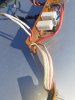
Ups! May be this is a part of the problem .Broken cable this time on rail wire connection20220718_171828.jpg 20220718_171836.jpg to GWX-594 Right driver plate,
These Pioneer wires are absolute garbage. Apparently they are made stiff and inelastic because of the ripping assembly, which was applied to save solder and soldering time. These wires are mounted on long pins due to the ripping assembly and both break and crack the solder joints of the pins in the boards because the pin acts as a lever. I really want to replace all those stiff stupid cables with flexible quality car cables with nice insulation and solder them.One day...
 
Last edited:
Yes, confirmation.

initial conditions:
VR1 = VR2 = VR3 = VR4 = fully ccw = zero ohms

for VR3, measurements of Q29 (base) & Q31 (base) for VR3(0k, 25k, 50k, 75k, 100k)
This is the correctly functioning left channel. It is a baseline comparison. +1.8v and -1.8v at their bases.

for VR4 measurements of Q30 (base) & Q32 (base) for VR4(0k, 25k, 50k, 75k, 100k)
this is the too hot right channel. This is troubleshooting. voltages should be similar to the left channel at.+1.8v and -1.8v NOT +4.7v and -4.7v

we don't need to repeat and repeat the GWH-593 Q1 & Q3 measurements, nor the GWH-594 Q2 & Q4, nor the empty output transistor positions.
The Q29, Q31, Q30 & Q32 measurements will show the needed data.

"IF, with VR1 & VR2 fully CCW varying VR3 and VR4 has no measurable effect TRY changing VR1 & VR2 to 25, then 50 ohms, to try to find conditions where VR3 & VR4 have measurable effects." Where to measure the effect of turning this VR and what is the target numbers?

Measure at Q29, Q31, Q30 & Q32, their base voltage. what is the target numbers,
the bad readings are +/- 4.7v as read when you did the VR2 test,
versus the correct reading of +/- 1.8 as read when you did the VR1 test
we are looking for ANY CHANGES in the reading when the VR3 is increased..

The readings CHANGED when VR1 was adjusted. Had we been measuring idle current, while VR1 was increasing, there would have been no change until the reading was big enough to overcome the Vbe turn on voltages of the drivers and outputs and allow the idle current to flow.

This type of situation may also exist with the VR3 & VR4 readings, increasing their resistance does not change the reading until a threshold (Q19? Q23?) is overcome.
 
Last edited:
Yes, confirmation.

initial conditions:
VR1 = VR2 = VR3 = VR4 = fully ccw = zero ohms

for VR3, measurements of Q29 (base) & Q31 (base) for VR3(0k, 25k, 50k, 75k, 100k)
This is the correctly functioning left channel. It is a baseline comparison. +1.8v and -1.8v at their bases.

for VR4 measurements of Q30 (base) & Q32 (base) for VR4(0k, 25k, 50k, 75k, 100k)
this is the too hot right channel. This is troubleshooting. voltages should be similar to the left channel at.+1.8v and -1.8v NOT +4.7v and -4.7v

we don't need to repeat and repeat the GWH-593 Q1 & Q3 measurements, nor the GWH-594 Q2 & Q4, nor the empty output transistor positions.
The Q29, Q31, Q30 & Q32 measurements will show the needed data.


Measure at Q29, Q31, Q30 & Q32, their base voltage. what is the target numbers,
the bad readings are +/- 4.7v as read when you did the VR2 test,
versus the correct reading of +/- 1.8 as read when you did the VR1 test
we are looking for ANY CHANGES in the reading when the VR3 is increased..

The readings CHANGED when VR1 was adjusted. Had we been measuring idle current, while VR1 was increasing, there would have been no change until the reading was big enough to overcome the Vbe turn on voltages of the drivers and outputs and allow the idle current to flow.

This type of situation may also exist with the VR3 & VR4 readings, increasing their resistance does not change the reading until a threshold (Q19? Q23?) is overcome.
Understood . I will proceed #78 in the day time. Know is too late. I re soldered the cable and make just quick measurement on the driver plates. Looks better know. But let see the digits.
 
20220719_210309.jpg
Yes, confirmation.

initial conditions:
VR1 = VR2 = VR3 = VR4 = fully ccw = zero ohms

for VR3, measurements of Q29 (base) & Q31 (base) for VR3(0k, 25k, 50k, 75k, 100k)
This is the correctly functioning left channel. It is a baseline comparison. +1.8v and -1.8v at their bases.

for VR4 measurements of Q30 (base) & Q32 (base) for VR4(0k, 25k, 50k, 75k, 100k)
this is the too hot right channel. This is troubleshooting. voltages should be similar to the left channel at.+1.8v and -1.8v NOT +4.7v and -4.7v

we don't need to repeat and repeat the GWH-593 Q1 & Q3 measurements, nor the GWH-594 Q2 & Q4, nor the empty output transistor positions.
The Q29, Q31, Q30 & Q32 measurements will show the needed data.


Measure at Q29, Q31, Q30 & Q32, their base voltage. what is the target numbers,
the bad readings are +/- 4.7v as read when you did the VR2 test,
versus the correct reading of +/- 1.8 as read when you did the VR1 test
we are looking for ANY CHANGES in the reading when the VR3 is increased..

The readings CHANGED when VR1 was adjusted. Had we been measuring idle current, while VR1 was increasing, there would have been no change until the reading was big enough to overcome the Vbe turn on voltages of the drivers and outputs and allow the idle current to flow.

This type of situation may also exist with the VR3 & VR4 readings, increasing their resistance does not change the reading until a threshold (Q19? Q23?) is overcome.

I start to do the measurements , but Just informative : VR3 and VR4 both 100K Ohms. on the board in circuit the resistance is from 0.5 Ohms to 40K Ohms and is possible to be measured only with arrow meter but not with a digital. So adjustment on 50K.75K, 100K is not possible So I ken do 0 Ohms 25K and 40K. It is OK?
I don't know why this picture goes too small.
 
Last edited:
You can't see the true resistance of VR3 and VR4 in circuit because they are in-circuit and other components around them are skewing your measurement. The 25k, 50k and 75k resistances will be at 1/4 turn, 1/2 turn and 3/4 turn positions.
 
View attachment 2619556

I start to do the measurements , but Just informative : VR3 and VR4 both 100K Ohms. on the board in circuit the resistance is from 0.5 Ohms to 40K Ohms and is possible to be measured only with arrow meter but not with a digital. So adjustment on 50K.75K, 100K is not possible So I ken do 0 Ohms 25K and 40K. It is OK?
I don't know why this picture goes too small.
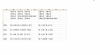
This may be is better visible Untitled.png
 
Yes, that is better.

The left and right channel voltages are very similar, the excessive heating you noticed should be gone.

The (formerly) elevated Q30 & Q32 base voltages ( +4.69v & -4.7v) were the clue. Another clue about them is that as VR2 was varied, they did not change.
This was part of the post #67 data.

Just in case, I gotta ask; When doing ohmmeter readings, the power is turned off?

Right now, that board doesn't seem to have any problems, the driver (base) voltage was at an appropriate level, on both channels.
the driver (base) voltage increased as VR1 (or VR2) was increased. It also increased as VR3 (or VR4) was increased.
 
Back
Top Bottom